SNLS334G April 2011 – January 2015 DS80PCI800
PRODUCTION DATA.
- 1 Features
- 2 Applications
- 3 Description
- 4 Revision History
- 5 Pin Configuration and Functions
- 6 Specifications
- 7 Parameter Measurement Information
- 8 Detailed Description
- 9 Application and Implementation
- 10Power Supply Recommendations
- 11Layout
- 12Device and Documentation Support
- 13Mechanical, Packaging, and Orderable Information
Package Options
Mechanical Data (Package|Pins)
- NJY|54
Thermal pad, mechanical data (Package|Pins)
Orderable Information
9 Application and Implementation
NOTE
Information in the following applications sections is not part of the TI component specification, and TI does not warrant its accuracy or completeness. TI’s customers are responsible for determining suitability of components for their purposes. Customers should validate and test their design implementation to confirm system functionality.
9.1 Application Information
9.1.1 DS80PCI800 versus DS80PCI810
The DS80PCI800 and DS80PCI810 are pin compatible, and both can be used for PCIe Gen-1, 2, and 3 applications. The DS80PCI800 is ideal for closed PCIe systems where significant insertion losses (> 35 dB at 4 GHz) are expected in the signal path. A closed system is defined as a PCIe environment with a limited number of possible Host-to-Endpoint combinations. The DS80PCI800 can extend the reach of a PCIe system by up to 36 dB beyond the max allowable PCIe channel loss, whereas the DS80PCI810 can extend the system range up to 10 dB while offering a larger dynamic range on output linearity. Due to the larger CTLE gain, the DS80PCI800 is able to compensate insertion loss over longer transmission lines before the repeater. In addition, the DS80PCI800 is able to produce de-emphasis levels up to -12 dB to support significant trace losses after the repeater (-15 dB at 4 GHz).
9.1.2 Signal Integrity in PCIe Applications
In PCIe Gen-3 applications, the specification requires Rx-Tx link training to establish and optimize signal conditioning settings at 8 Gbps. In link training, the Rx partner requests a series of FIR - preshoot and de-emphasis coefficients (10 Presets) from the Tx partner. The Rx partner includes 7-levels (6 dB to 12 dB) of CTLE followed by a single tap DFE. The link training would pre-condition the signal with an equalized link between the root-complex and endpoint. Note that there is no link training in PCIe Gen-1 (2.5 Gbps) or PCIe Gen-2 (5.0 Gbps) applications. The DS80PCI800 is placed in between the Tx and Rx. It would help extend the PCB trace reach distance by boosting the attenuated signals with it's equalization, so that the signal can be more easily recovered by the downstream Rx. In Gen 3 mode, DS80PCI800 transmit outputs are designed to pass the Tx Preset signaling onto the Rx for the PCIe Gen 3 link to train and optimize the equalization settings. The suggested setting for the DS80PCI800 are EQ = 0x00, VOD = 1.2 Vp-p and DEM = 0 dB. Additional adjustments to increase the EQ or DEM setting should be performed to optimize the eye opening in the Rx partner. See the tables below for Pin Mode and SMBus Mode configurations.
Table 10. Suggested Device Settings in Pin Mode
| Channel | Pin Mode Settings |
|---|---|
| EQx[1:0] | 0, 0 (Level 1) |
| DEMx[1:0] | Float, R (Level 10) |
Table 11. Suggested Device Settings in SMBus Slave Mode
| Register | Write Value | Comments |
|---|---|---|
| 0x06 | 0x18 | Enables SMBus Slave Mode Register Control |
| 0x0F | 0x00 | Set CHB_0 EQ to 0x00. |
| 0x10 | 0xAD | Set CHB_0 VOD to 101'b (1.2 Vp-p). |
| 0x11 | 0x00 | Set CHB_0 DEM to 000'b (0 dB). |
| 0x16 | 0x00 | Set CHB_1 EQ to 0x00. |
| 0x17 | 0xAD | Set CHB_1 VOD to 101'b (1.2 Vp-p). |
| 0x18 | 0x00 | Set CHB_1 DEM to 000'b (0 dB). |
| 0x1D | 0x00 | Set CHB_2 EQ to 0x00. |
| 0x1E | 0xAD | Set CHB_2 VOD to 101'b (1.2 Vp-p). |
| 0x1F | 0x00 | Set CHB_2 DEM to 000'b (0 dB). |
| 0x24 | 0x00 | Set CHB_3 EQ to 0x00. |
| 0x25 | 0xAD | Set CHB_3 VOD to 101'b (1.2 Vp-p). |
| 0x26 | 0x00 | Set CHB_3 DEM to 000'b (0 dB). |
| 0x2C | 0x00 | Set CHA_0 EQ to 0x00. |
| 0x2D | 0xAD | Set CHA_0 VOD to 101'b (1.2 Vp-p). |
| 0x2E | 0x00 | Set CHA_0 DEM to 000'b (0 dB). |
| 0x33 | 0x00 | Set CHA_1 EQ to 0x00. |
| 0x34 | 0xAD | Set CHA_1 VOD to 101'b (1.2 Vp-p). |
| 0x35 | 0x00 | Set CHA_1 DEM to 000'b (0 dB). |
| 0x3A | 0x00 | Set CHA_2 EQ to 0x00. |
| 0x3B | 0xAD | Set CHA_2 VOD to 101'b (1.2 Vp-p). |
| 0x3C | 0x00 | Set CHA_2 DEM to 000'b (0 dB). |
| 0x41 | 0x00 | Set CHA_3 EQ to 0x00. |
| 0x42 | 0xAD | Set CHA_3 VOD to 101'b (1.2 Vp-p). |
| 0x43 | 0x00 | Set CHA_3 DEM to 000'b (0 dB). |
9.2 Typical Application
The DS80PCI800 extends PCB trace and cable reach in PCIe Gen1, 2 and 3 applications by applying equalization to compensate for the insertion loss of the trace or cable. In Gen 3 mode, the device aids specifically in the equalization link training to improve the margin and overall eye inside the Rx. The DS80PCI800 can be used on the motherboard, mid plane (riser card), end-point target cards, and active cable assemblies. The capability of the DS80PCI800 performance is shown in the following two test setup connections.
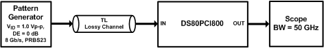 Figure 8. Test Setup 1 Connections Diagram
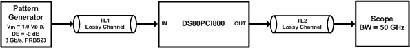 Figure 9. Test Setup 2 Connections Diagram
9.2.1 Design Requirements
As with any high speed design, there are many factors which influence the overall performance. The following list indicates critical areas for consideration during design.
- Use 100 Ω impedance traces. Length matching on the P and N traces should be done on the single-end segments of the differential pair.
- Use uniform trace width and trace spacing for differential pairs.
- Place AC-coupling capacitors near to the receiver end of each channel segment to minimize reflections.
- For Gen3, AC-coupling capacitors of 220 nF are recommended, maximum body size is 0402, and add cutout void on GND plane below the landing pad of the capacitor to reduce parasitic capacitance to GND.
- Back-drill connector vias and signal vias to minimize stub length.
- Use Reference plane vias to ensure a low inductance path for the return current.
9.2.2 Detailed Design Procedure
The DS80PCI800 should be placed at an offset location and close to the Rx with respect to the overall channel attenuation. The suggested settings are recommended as a starting point for most applications. Once these settings are configured, additional adjustments of the DS80PCI800 EQ or DE may be required to optimize the repeater performance. The CTLE and DFE coefficient in the Rx can also be adjusted to further improve the eye opening.
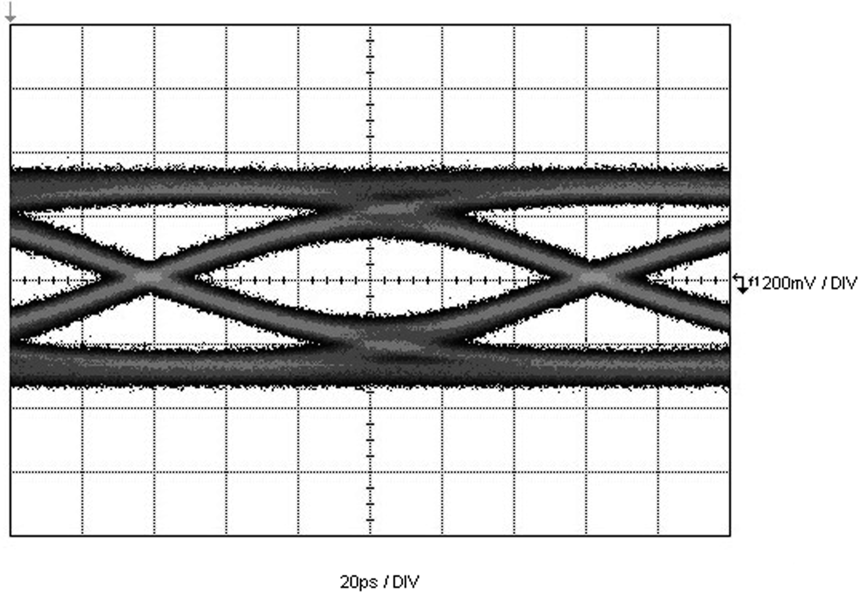
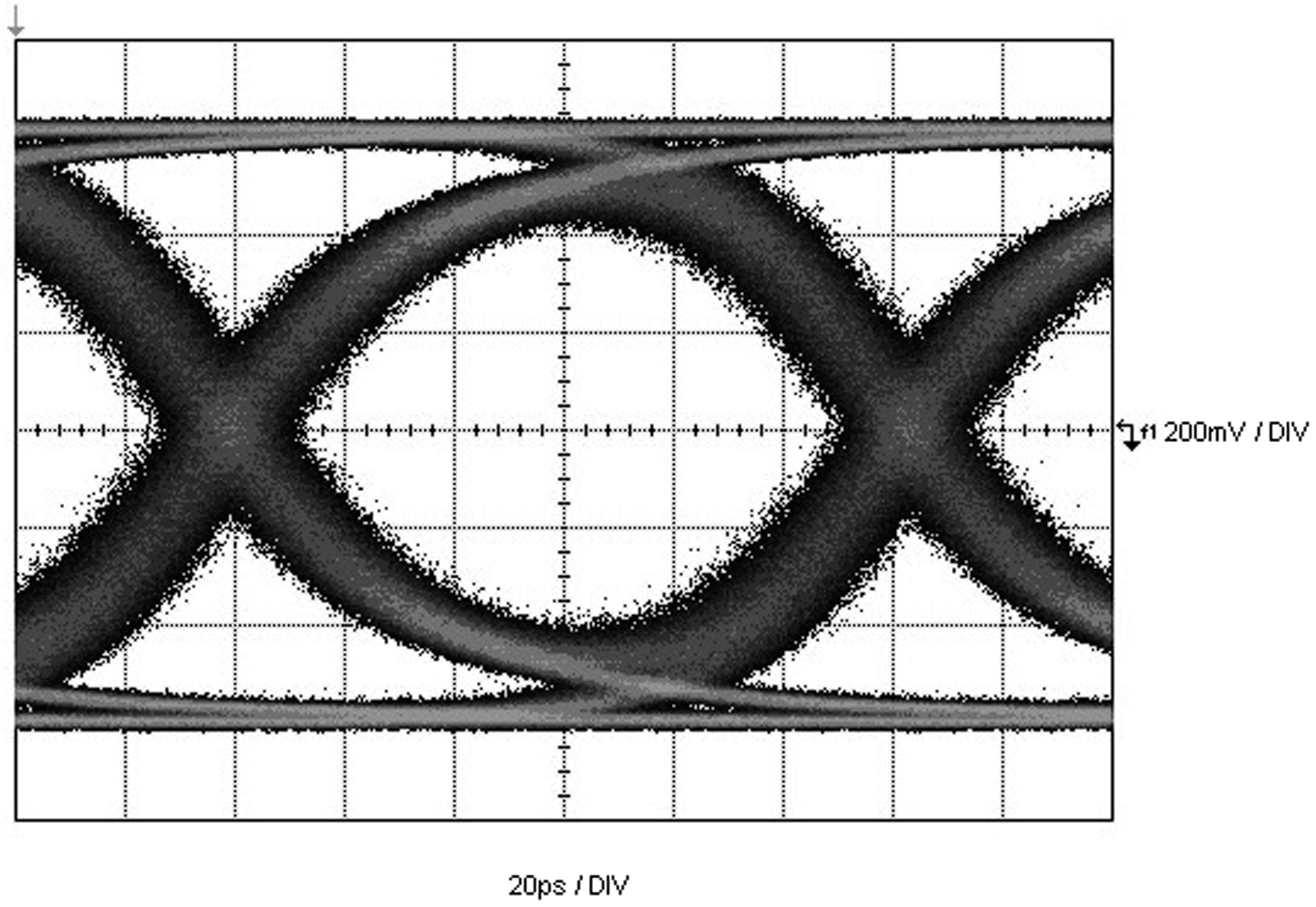
9.2.3 Application Curves
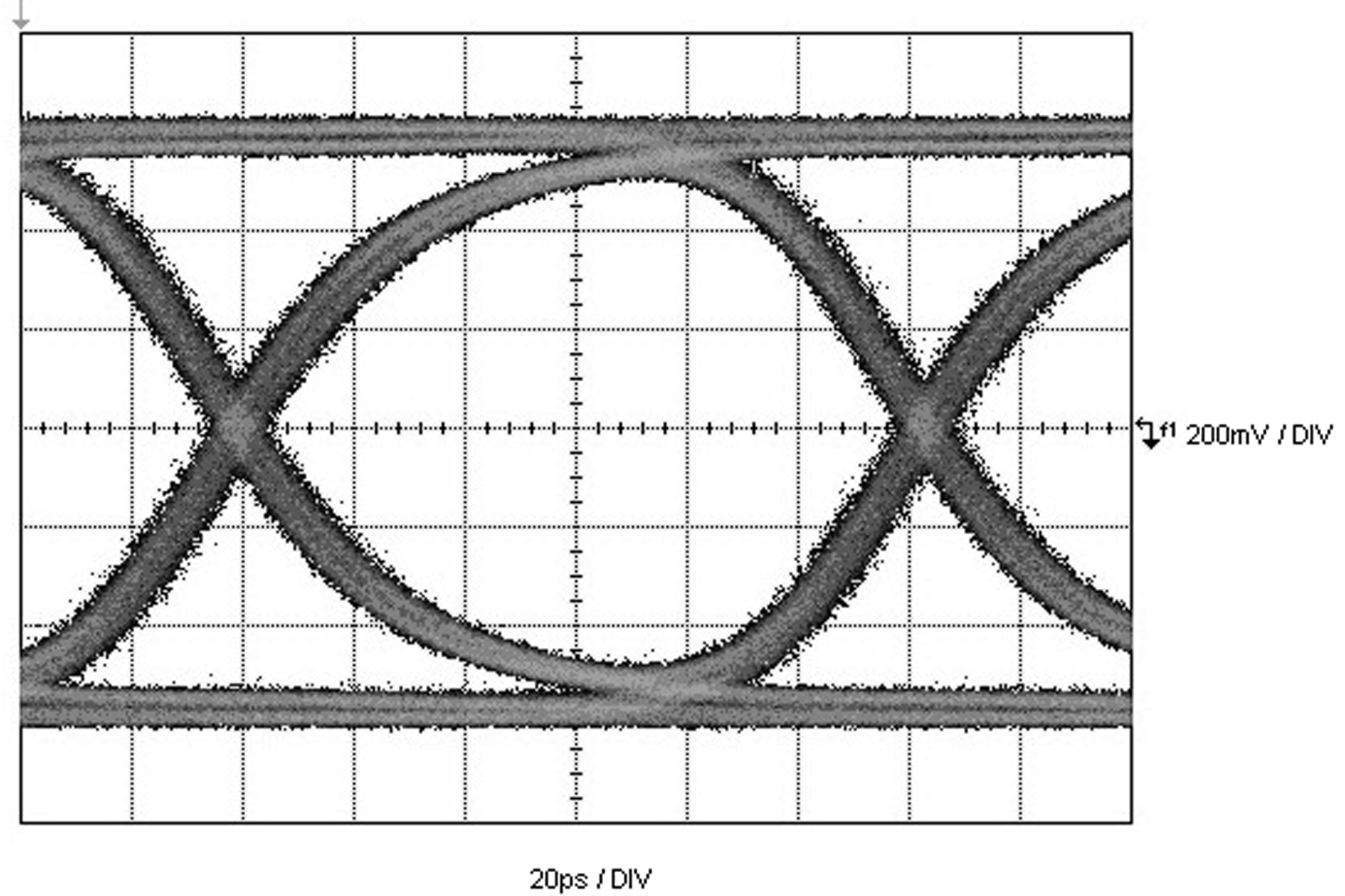
EQ[1:0] = [R, R] or 0x15, DEM[1:0] = [Float, Float]
EQ[1:0] = [R, R] or 0x15, DEM[1:0] = [Float, Float]
EQ[1:0] = [Float, R] or 0x1F, DEM[1:0] = [Float, Float]
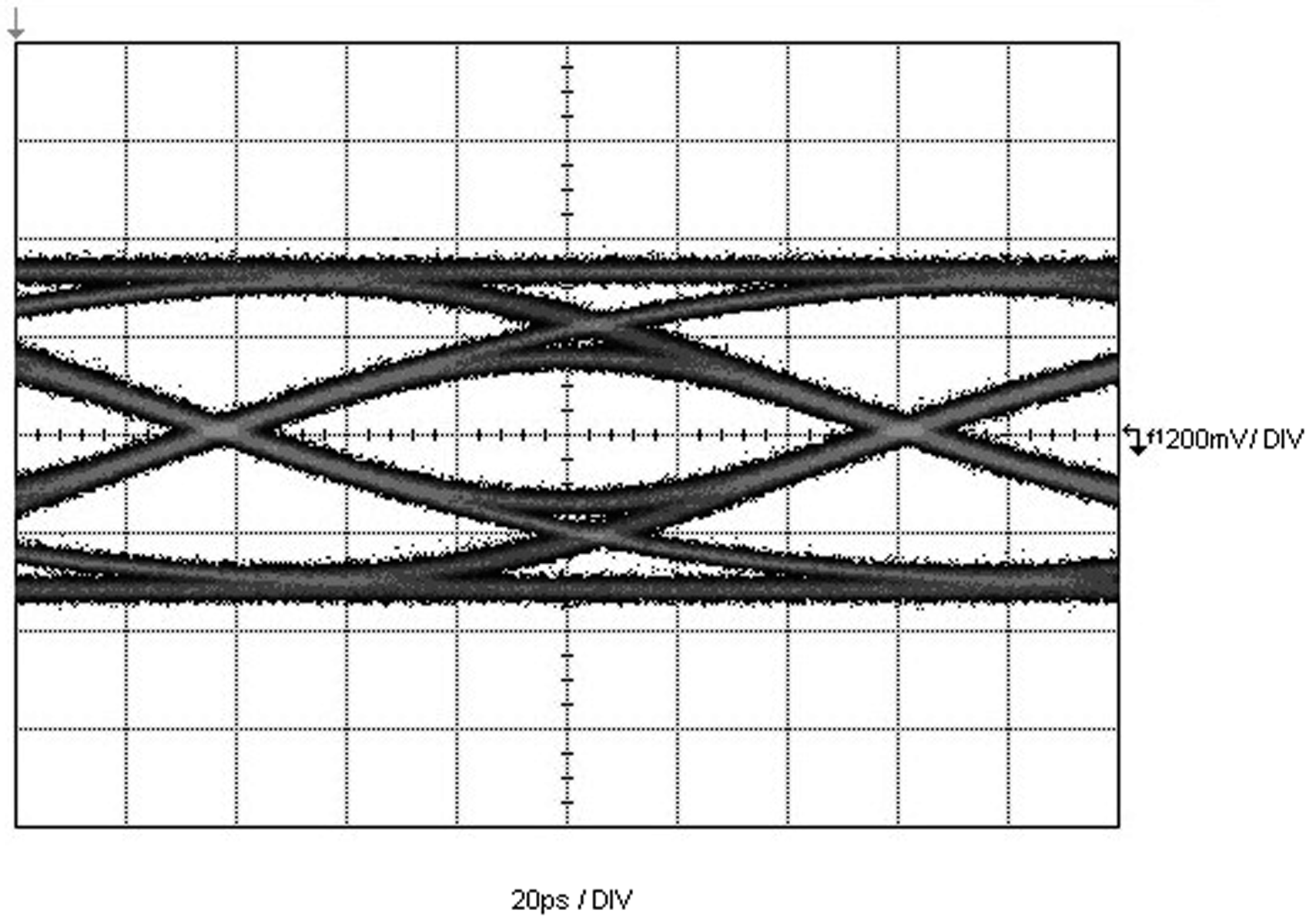
EQ[1:0] = [R, 1] or 0x0F, DEM[1:0] = [Float, Float]