SNLS334G April 2011 – January 2015 DS80PCI800
PRODUCTION DATA.
- 1 Features
- 2 Applications
- 3 Description
- 4 Revision History
- 5 Pin Configuration and Functions
- 6 Specifications
- 7 Parameter Measurement Information
- 8 Detailed Description
- 9 Application and Implementation
- 10Power Supply Recommendations
- 11Layout
- 12Device and Documentation Support
- 13Mechanical, Packaging, and Orderable Information
Package Options
Mechanical Data (Package|Pins)
- NJY|54
Thermal pad, mechanical data (Package|Pins)
Orderable Information
8 Detailed Description
8.1 Overview
The DS80PCI800 provides input CTLE and output De-emphasis equalization for lossy printed circuit board trace and cables. The DS80PCI800 operates in three modes: Pin Control Mode configuration (ENSMB = 0), SMBus Slave Mode (ENSMB = 1) for register configurations from host controller or SMBus Master Mode (ENSMB = Float) for loading the register configurations from an external EEPROM.
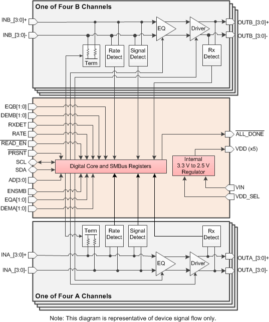
8.2 Functional Block Diagram
8.3 Feature Description
8.3.1 4-Level Input Configuration Guidelines
The 4-level input pins use a resistor divider to help set the four valid levels. There is an internal 30-kΩ pullup and a 60-kΩ pulldown connected to the package pin. These resistors, together with the external resistor connection combine to achieve the desired voltage level. Using the 1-kΩ pullup, 1-kΩ pulldown, no connect, or 20-kΩ pulldown provide the optimal voltage levels for each of the four input states.
Table 1. 4-Level Input Voltage
| LEVEL | SETTING | 3.3-V MODE | 2.5-V MODE | |
|---|---|---|---|---|
| 0 | 1 kΩ to GND | 0.1 V | 0.08 V | |
| R | 20 kΩ to GND | 0.33 × VIN | 0.33 × VDD | |
| F | FLOAT | 0.67 × VIN | 0.67 × VDD | |
| 1 | 1 kΩ to VDD/VIN | VIN – 0.05 V | VDD – 0.04 V | |
Typical 4-level input thresholds:
- Level 1 to 2 = 0.2 VIN or VDD
- Level 2 to 3 = 0.5 VIN or VDD
- Level 3 to 4 = 0.8 VIN or VDD
To minimize the start-up current associated with the integrated 2.5 V regulator, the 1-kΩ pullup and pulldown resistors are recommended. If several 4-level inputs require the same setting, it is possible to combine two or more 1-kΩ resistors into a single lower value resistor. As an example; combining two inputs with a single 500-Ω resistor is a good way to save board space. For the 20 kΩ to GND, this should also scale to 10 kΩ.
Table 2. Equalizer Settings(1)
| EQUALIZATION BOOST RELATIVE TO DC | |||||||
|---|---|---|---|---|---|---|---|
| LEVEL | EQA1 EQB1 |
EQA0 EQB0 |
EQ – 8 BITS [7:0] | dB at 1.25 GHz |
dB at 2.5 GHz |
dB at 4 GHz |
SUGGESTED USE |
| 1 | 0 | 0 | 0000 0000 = 0x00 | 2.1 | 3.7 | 4.9 | FR4 < 5 inch trace |
| 2 | 0 | R | 0000 0001 = 0x01 | 3.4 | 5.8 | 7.9 | FR4 5 inch 5–mil trace |
| 3 | 0 | Float | 0000 0010 = 0x02 | 4.8 | 7.7 | 9.9 | FR4 5 inch 4-mil trace |
| 4 | 0 | 1 | 0000 0011 = 0x03 | 5.9 | 8.9 | 11.0 | FR4 10 inch 5–mil trace |
| 5 | R | 0 | 0000 0111 = 0x07 | 7.2 | 11.2 | 14.3 | FR4 10 inch 4-mil trace |
| 6 | R | R | 0001 0101 = 0x15 | 6.1 | 11.4 | 14.6 | FR4 15 inch 4-mil trace |
| 7 | R | Float | 0000 1011 = 0x0B | 8.8 | 13.5 | 17.0 | FR4 20 inch 4-mil trace |
| 8 | R | 1 | 0000 1111 = 0x0F | 10.2 | 15.0 | 18.5 | FR4 25 to 30 inch 4-mil trace |
| 9 | Float | 0 | 0101 0101 = 0x55 | 7.5 | 12.8 | 18.0 | FR4 30 inch 4-mil trace |
| 10 | Float | R | 0001 1111 = 0x1F | 11.4 | 17.4 | 22.0 | FR4 35 inch 4-mil trace |
| 11 | Float | Float | 0010 1111 = 0x2F | 13.0 | 19.7 | 24.4 | 10 m, 30-awg cable |
| 12 | Float | 1 | 0011 1111 = 0x3F | 14.2 | 21.1 | 25.8 | 10 m – 12m cable |
| 13 | 1 | 0 | 1010 1010 = 0xAA | 13.8 | 21.7 | 27.4 | |
| 14 | 1 | R | 0111 1111 = 0x7F | 15.6 | 23.5 | 29.0 | |
| 15 | 1 | Float | 1011 1111 = 0xBF | 17.2 | 25.8 | 31.4 | |
| 16 | 1 | 1 | 1111 1111 = 0xFF | 18.4 | 27.3 | 32.7 | |
Table 3. Output Voltage and De-Emphasis Settings(1)
| LEVEL | DEMA1 DEMB1 |
DEMA0 DEMB0 |
VOD Vp-p | DEM dB(1) | INNER AMPLITUDE Vp-p |
SUGGESTED USE |
|---|---|---|---|---|---|---|
| 1 | 0 | 0 | 0.8 | 0 | 0.8 | FR4 < 5 inch 4-mil trace |
| 2 | 0 | R | 0.9 | 0 | 0.9 | FR4 < 5 inch 4-mil trace |
| 3 | 0 | Float | 0.9 | –3.5 | 0.6 | FR4 10 inch 4-mil trace |
| 4 | 0 | 1 | 1.0 | 0 | 1.0 | FR4 < 5 inch 4-mil trace |
| 5 | R | 0 | 1.0 | –3.5 | 0.7 | FR4 10 inch 4-mil trace |
| 6 | R | R | 1.0 | –6 | 0.5 | FR4 15 inch 4-mil trace |
| 7 | R | Float | 1.1 | 0 | 1.1 | FR4 < 5 inch 4-mil trace |
| 8 | R | 1 | 1.1 | –3.5 | 0.7 | FR4 10 inch 4-mil trace |
| 9 | Float | 0 | 1.1 | –6 | 0.6 | FR4 15 inch 4-mil trace |
| 10 | Float | R | 1.2 | 0 | 1.2 | FR4 < 5 inch 4-mil trace |
| 11 | Float | Float | 1.2 | –3.5 | 0.8 | FR4 10 inch 4-mil trace |
| 12 | Float | 1 | 1.2 | –6 | 0.6 | FR4 15 inch 4-mil trace |
| 13 | 1 | 0 | 1.3 | 0 | 1.3 | FR4 < 5 inch 4-mil trace |
| 14 | 1 | R | 1.3 | –3.5 | 0.9 | FR4 10 inch 4-mil trace |
| 15 | 1 | Float | 1.3 | –6 | 0.7 | FR4 15 inch 4-mil trace |
| 16 | 1 | 1 | 1.3 | –9 | 0.5 | FR4 20 inch 4-mil trace |
The de-emphasis levels are available in GEN1, GEN2, and GEN 3 modes when RATE = Float.
Table 4. RX-Detect Settings
| PRSNT(1)
(PIN 52) |
RXDET (PIN 22) |
SMBus REG BIT[3:2] |
INPUT TERMINATION | COMMENTS |
|---|---|---|---|---|
| 0 | 0 | 00 | Hi-Z | Manual RX-Detect, input is high-impedance mode |
| 0 | Tie 20 kΩ to GND |
01 | Pre Detect: Hi-Z Post Detect: 50 Ω |
Auto RX-Detect, outputs test every 12 ms for 600 ms then stops; termination is hi-Z until detection; once detected input termination is 50 Ω Reset function by pulsing PRSNT high for 5 µs then low again |
| 0 | Float (Default) |
10 | Pre Detect: Hi-Z Post Detect: 50 Ω |
Auto RX-Detect, outputs test every 12 ms until detection occurs; termination is hi-Z until detection; once detected input termination is 50 Ω Reset function by pulsing PRSNT high for 5 µs then low again |
| 0 | 1 | 11 | 50 Ω | Manual RX-Detect, input is 50 Ω |
| 1 | X | Hi-Z | Power-down mode, input is high impedance, output drivers are disabled Used to reset RX-Detect State Machine when held high for 5 µs |
Table 5. Signal Detect Threshold Level(1)
| SD_TH | SMBus REG BIT [3:2] AND [1:0] | ASSERT LEVEL (TYP) | DEASSERT LEVEL (TYP) |
|---|---|---|---|
| 0 | 10 | 210 mVp-p | 150 mVp-p |
| R | 01 | 160 mVp-p | 100 mVp-p |
| F (default) | 00 | 180 mVp-p | 110 mVp-p |
| 1 | 11 | 190 mVp-p | 130 mVp-p |
8.4 Device Functional Modes
The DS80PCI800 is a low-power 8-channel repeater optimized for PCI Express Gen 1/2 and 3. The DS80PCI800 compensates for lossy FR-4 printed circuit board backplanes and balanced cables. The DS80PCI800 operates in three modes: Pin Control Mode (ENSMB = 0), SMBus Slave Mode (ENSMB = 1) and SMBus Master Mode (ENSMB = float) to load register information from external EEPROM; refer to SMBus Master Mode for additional information.
8.4.1 Pin Control Mode
When in pin mode (ENSMB = 0), equalization and de-emphasis can be selected via pin for each side independently. When de-emphasis is asserted VOD is automatically adjusted per the De- Emphasis table below. The RXDET pins provides automatic and manual control for input termination (50 Ω or > 50 kΩ). RATE setting is also pin controllable with pin selections (Gen 1/2, auto detect and Gen 3). The receiver electrical idle detect threshold is also adjustable via the SD_TH pin.
8.4.2 SMBUS Mode
When in SMBus mode (ENSMB = 1), the VOD (output amplitude), equalization, de-emphasis, and termination disable features are all programmable on a individual lane basis, instead of grouped by A or B as in the pin mode case. Upon assertion of ENSMB, the EQx and DEMx functions revert to register control immediately. The EQx and DEMx pins are converted to AD0-AD3 SMBus address inputs. The other external control pins (RATE, RXDET and SD_TH) remain active unless their respective registers are written to and the appropriate override bit is set, in which case they are ignored until ENSMB is driven low (pin mode). On power-up and when ENSMB is driven low all registers are reset to their default state. If PRSNT is asserted while ENSMB is high, the registers retain their current state.
Equalization settings accessible via the pin controls were chosen to meet the needs of most PCIe applications. If additional fine tuning or adjustment is needed, additional equalization settings can be accessed via the SMBus registers. Each input has a total of 256 possible equalization settings. The 4-Level Input Configuration Guidelines show the 16 setting when the device is in pin mode. When using SMBus mode, the equalization, VOD and de-emphasis levels are set by registers.
8.5 Programming
8.5.1 System Management Bus (SMBus) and Configuration Registers
The System Management Bus interface is compatible to SMBus 2.0 physical layer specification. ENSMB = 1 kΩ to VDD to enable SMBus slave mode and allow access to the configuration registers.
The DS80PCI800 has the AD[3:0] inputs in SMBus mode. These pins are the user set SMBUS slave address inputs. The AD[3:0] pins have internal pulldown. When left floating or pulled low the AD[3:0] = 0000'b, the device default address byte is 0xB0. Based on the SMBus 2.0 specification, the DS80PCI800 has a 7-bit slave address. The LSB is set to 0'b (for a WRITE). The device supports up to 16 address byte, which can be set with the AD[3:0] inputs. Below are the 16 addresses.
Table 6. Device Slave Address Bytes
| AD[3:0] SETTINGS | ADDRESS BYTES (HEX) | 7-BIT SLAVE ADDRESS (HEX) |
|---|---|---|
| 0000 | B0 | 58 |
| 0001 | B2 | 59 |
| 0010 | B4 | 5A |
| 0011 | B6 | 5B |
| 0100 | B8 | 5C |
| 0101 | BA | 5D |
| 0110 | BC | 5E |
| 0111 | BE | 5F |
| 1000 | C0 | 60 |
| 1001 | C2 | 61 |
| 1010 | C4 | 62 |
| 1011 | C6 | 63 |
| 1100 | C8 | 64 |
| 1101 | CA | 65 |
| 1110 | CC | 66 |
| 1111 | CE | 67 |
The SDA/SCL pins are 3.3 V tolerant, but are not 5 V tolerant. An external pullup resistor is required on the SDA and SCL line. The resistor value can be from 2 kΩ to 5 kΩ depending on the voltage, loading, and speed.
8.5.2 Transfer of Data Through the SMBus
During normal operation the data on SDA must be stable during the time when SCL is High.
There are three unique states for the SMBus:
START: A high-to-low transition on SDA while SCL is High indicates a message START condition.
STOP: A low-to-high transition on SDA while SCL is High indicates a message STOP condition.
IDLE: If SCL and SDA are both High for a time exceeding tBUF from the last detected STOP condition or if they are High for a total exceeding the maximum specification for tHIGH then the bus will transfer to the IDLE state.
8.5.3 Writing a Register
To write a register, the following protocol is used (see SMBus 2.0 specification).
- The Host drives a START condition, the 7-bit SMBus address, and a “0” indicating a WRITE.
- The Device (Slave) drives the ACK bit (“0”).
- The Host drives the 8-bit Register Address.
- The Device drives an ACK bit (“0”).
- The Host drive the 8-bit data byte.
- The Device drives an ACK bit (“0”).
- The Host drives a STOP condition.
The WRITE transaction is completed, the bus goes IDLE and communication with other SMBus devices may now occur.
8.5.4 Reading a Register
To read a register, the following protocol is used (see SMBus 2.0 specification).
- The Host drives a START condition, the 7-bit SMBus address, and a “0” indicating a WRITE.
- The Device (Slave) drives the ACK bit (“0”).
- The Host drives the 8-bit Register Address.
- The Device drives an ACK bit (“0”).
- The Host drives a START condition.
- The Host drives the 7-bit SMBus Address, and a “1” indicating a READ.
- The Device drives an ACK bit “0”.
- The Device drives the 8-bit data value (register contents).
- The Host drives a NACK bit “1”indicating end of the READ transfer.
- The Host drives a STOP condition.
The READ transaction is completed, the bus goes IDLE and communication with other SMBus devices may now occur.
8.5.5 SMBus Master Mode
The DS80PCI800 device supports reading directly from an external EEPROM device by implementing SMBus Master mode. When using the SMBus master mode, the DS80PCI800 will read directly from specific location in the external EEPROM. When designing a system for using the external EEPROM, the user needs to follow these specific guidelines.
- Set ENSMB = Float — enable the SMBUS master mode.
- The external EEPROM device address byte must be 0xA0 and capable of 1 MHz operation at 2.5 V and 3.3 V supply. The maximum allowed size is 8 kbits (1024 bytes).
- Set the AD[3:0] inputs for SMBus address byte. When the AD[3:0] = 0000'b, the device address byte is 0xB0.
When tying multiple DS80PCI800 devices to the SDA and SCL bus, use these guidelines to configure the devices.
- Use SMBus AD[3:0] address bits so that each device can loaded its configuration from the EEPROM. Example below is for 4 devices.
- U1: AD[3:0] = 0000 = 0xB0
- U2: AD[3:0] = 0001 = 0xB2
- U3: AD[3:0] = 0010 = 0xB4
- U4: AD[3:0] = 0011 = 0xB6
- Use a pullup resistor on SDA and SCL; value = 2 kΩ
- Daisy-chain READ_EN (pin 26) and ALL_DONE (pin 27) from one device to the next device in the sequence so that they do not compete for the EEPROM at the same time.
- Tie READ_EN of the first device in the chain (U1) to GND
- Tie ALL_DONE of U1 to READ_EN of U2
- Tie ALL_DONE of U2 to READ_EN of U3
- Tie ALL_DONE of U3 to READ_EN of U4
- Optional: Tie ALL_DONE output of U4 to a LED to show the devices have been loaded successfully
The following example represents a 2 kbits (256 × 8-bit) EEPROM in hex format for the DS80PCI800 device. The first 3 bytes of the EEPROM always contain a header common and necessary to control initialization of all devices connected to the SMBus. CRC enable flag to enable/disable CRC checking. If CRC checking is disabled, a fixed pattern (0xA5) is written/read instead of the CRC byte from the CRC location, to simplify the control. There is a MAP bit to flag the presence of an address map that specifies the configuration data start in the EEPROM. If the MAP bit is not present the configuration data start address is derived from the DS80PCI800 address and the configuration data size. A bit to indicate an EEPROM size > 256 bytes is necessary to properly address the EEPROM. There are 37 bytes of data size for each DS80PCI800 device.
:2000000000001000000407002FAD4002FAD4002FAD4002FAD401805F5A8005F5A8005F5AD8
:200020008005F5A800005454000000000000000000000000000000000000000000000000F6
:20006000000000000000000000000000000000000000000000000000000000000000000080
:20008000000000000000000000000000000000000000000000000000000000000000000060
:2000A000000000000000000000000000000000000000000000000000000000000000000040
:2000C000000000000000000000000000000000000000000000000000000000000000000020
:2000E000000000000000000000000000000000000000000000000000000000000000000000
:200040000000000000000000000000000000000000000000000000000000000000000000A0
For more information in regards to EEPROM programming and the hex format, see SNLA228.
8.6 Register Maps
Table 7. EEPROM Register Map - Single Device with Default Value
| EEPROM Address Byte | Bit 7 | Bit 6 | Bit 5 | Bit 4 | Bit 3 | Bit 2 | Bit 1 | BIt 0 | ||
|---|---|---|---|---|---|---|---|---|---|---|
| Description | 0x00 | CRC EN | Address Map Present | EEPROM > 256 Bytes | RES | DEVICE COUNT[3] | DEVICE COUNT[2] | DEVICE COUNT[1] | DEVICE COUNT[0] | |
| Default Value | 0x00 | 0 | 0 | 0 | 0 | 0 | 0 | 0 | 0 | |
| Description | 0x01 | RES | RES | RES | RES | RES | RES | RES | RES | |
| Default Value | 0x00 | 0 | 0 | 0 | 0 | 0 | 0 | 0 | 0 | |
| Description | 0x02 | Max EEPROM Burst size[7] | Max EEPROM Burst size[6] | Max EEPROM Burst size[5] | Max EEPROM Burst size[4] | Max EEPROM Burst size[3] | Max EEPROM Burst size[2] | Max EEPROM Burst size[1] | Max EEPROM Burst size[0] | |
| Default Value | 0x00 | 0 | 0 | 0 | 0 | 0 | 0 | 0 | 0 | |
| Description | 0x03 | PWDN_ch7 | PWDN_ch6 | PWDN_ch5 | PWDN_ch4 | PWDN_ch3 | PWDN_ch2 | PWDN_ch1 | PWDN_ch0 | |
| SMBus Register | 0x01[7] | 0x01[6] | 0x01[5] | 0x01[4] | 0x01[3] | 0x01[2] | 0x01[1] | 0x01[0] | ||
| Default Value | 0x00 | 0 | 0 | 0 | 0 | 0 | 0 | 0 | 0 | |
| Description | 0x04 | lpbk_1 | lpbk_0 | PWDN_INPUTS | PWDN_OSC | Ovrd_PRSNT | RES | RES | RES | |
| SMBus Register | 0x02[5] | 0x02[4] | 0x02[3] | 0x02[2] | 0x02[0] | 0x04[7] | 0x04[6] | 0x04[5] | ||
| Default Value | 0x00 | 0 | 0 | 0 | 0 | 0 | 0 | 0 | 0 | |
| Description | 0x05 | RES | RES | RES | RES | RES | rxdet_btb_en | Ovrd_idle_th | Ovrd_RES | |
| SMBus Register | 0x04[4] | 0x04[3] | 0x04[2] | 0x04[1] | 0x04[0] | 0x06[4] | 0x08[6] | 0x08[5] | ||
| Default Value | 0x04 | 0 | 0 | 0 | 0 | 0 | 1 | 0 | 0 | |
| Description | 0x06 | Ovrd_IDLE | Ovrd_RX_DET | Ovrd_RATE | RES | RES | rx_delay_sel_2 | rx_delay_sel_1 | rx_delay_sel_0 | |
| SMBus Register | 0x08[4] | 0x08[3] | 0x08[2] | 0x08[1] | 0x08[0] | 0x0B[6] | 0x0B[5] | 0x0B[4] | ||
| Default Value | 0x07 | 0 | 0 | 0 | 0 | 0 | 1 | 1 | 1 | |
| Description | 0x07 | RD_delay_sel_3 | RD_delay_sel_2 | RD_delay_sel_1 | RD_delay_sel_0 | ch0_Idle_auto | ch0_Idle_sel | ch0_RXDET_1 | ch0_RXDET_0 | |
| SMBus Register | 0x0B[3] | 0x0B[2] | 0x0B[1] | 0x0B[0] | 0x0E[5] | 0x0E[4] | 0x0E[3] | 0x0E[2] | ||
| Default Value | 0x00 | 0 | 0 | 0 | 0 | 0 | 0 | 0 | 0 | |
| Description | 0x08 | ch0_BST_7 | ch0_BST_6 | ch0_BST_5 | ch0_BST_4 | ch0_BST_3 | ch0_BST_2 | ch0_BST_1 | ch0_BST_0 | |
| SMBus Register | 0x0F[7] | 0x0F[6] | 0x0F[5] | 0x0F[4] | 0x0F[3] | 0x0F[2] | 0x0F[1] | 0x0F[0] | ||
| Default Value | 0x2F | 0 | 0 | 1 | 0 | 1 | 1 | 1 | 1 | |
| Description | 0x09 | ch0_Sel_scp | ch0_Sel_mode | ch0_RES_2 | ch0_RES_1 | ch0_RES_0 | ch0_VOD_2 | ch0_VOD_1 | ch0_VOD_0 | |
| SMBus Register | 0x10[7] | 0x10[6] | 0x10[5] | 0x10[4] | 0x10[3] | 0x10[2] | 0x10[1] | 0x10[0] | ||
| Default Value | 0xAD | 1 | 0 | 1 | 0 | 1 | 1 | 0 | 1 | |
| Description | 0x0A | ch0_DEM_2 | ch0_DEM_1 | ch0_DEM_0 | ch0_Slow | ch0_idle_tha_1 | ch0_idle_tha_0 | ch0_idle_thd_1 | ch0_idle_thd_0 | |
| SMBus Register | 0x11[2] | 0x11[1] | 0x11[0] | 0x12[7] | 0x12[3] | 0x12[2] | 0x12[1] | 0x12[0] | ||
| Default Value | 0x40 | 0 | 1 | 0 | 0 | 0 | 0 | 0 | 0 | |
| Description | 0x0B | ch1_Idle_auto | ch1_Idle_sel | ch1_RXDET_1 | ch1_RXDET_0 | ch1_BST_7 | ch1_BST_6 | ch1_BST_5 | ch1_BST_4 | |
| SMBus Register | 0x15[5] | 0x15[4] | 0x15[3] | 0x15[2] | 0x16[7] | 0x16[6] | 0x16[5] | 0x16[4] | ||
| Default Value | 0x02 | 0 | 0 | 0 | 0 | 0 | 0 | 1 | 0 | |
| Description | 0x0C | ch1_BST_3 | ch1_BST_2 | ch1_BST_1 | ch1_BST_0 | ch1_Sel_scp | ch1_Sel_mode | ch1_RES_2 | ch1_RES_1 | |
| SMBus Register | 0x16[3] | 0x16[2] | 0x16[1] | 0x16[0] | 0x17[7] | 0x17[6] | 0x17[5] | 0x17[4] | ||
| Default Value | 0xFA | 1 | 1 | 1 | 1 | 1 | 0 | 1 | 0 | |
| Description | 0x0D | ch1_RES_0 | ch1_VOD_2 | ch1_VOD_1 | ch1_VOD_0 | ch1_DEM_2 | ch1_DEM_1 | ch1_DEM_0 | ch1_Slow | |
| SMBus Register | 0x17[3] | 0x17[2] | 0x17[1] | 0x17[0] | 0x18[2] | 0x18[1] | 0x18[0] | 0x19[7] | ||
| Default Value | 0xD4 | 1 | 1 | 0 | 1 | 0 | 1 | 0 | 0 | |
| Description | 0x0E | ch1_idle_tha_1 | ch1_idle_tha_0 | ch1_idle_thd_1 | ch1_idle_thd_0 | ch2_Idle_auto | ch2_Idle_sel | ch2_RXDET_1 | ch2_RXDET_0 | |
| SMBus Register | 0x19[3] | 0x19[2] | 0x19[1] | 0x19[0] | 0x1C[5] | 0x1C[4] | 0x1C[3] | 0x1C[2] | ||
| Default Value | 0x00 | 0 | 0 | 0 | 0 | 0 | 0 | 0 | 0 | |
| Description | 0x0F | ch2_BST_7 | ch2_BST_6 | ch2_BST_5 | ch2_BST_4 | ch2_BST_3 | ch2_BST_2 | ch2_BST_1 | ch2_BST_0 | |
| SMBus Register | 0x1D[7] | 0x1D[6] | 0x1D[5] | 0x1D[4] | 0x1D[3] | 0x1D[2] | 0x1D[1] | 0x1D[0] | ||
| Default Value | 0x2F | 0 | 0 | 1 | 0 | 1 | 1 | 1 | 1 | |
| Description | 0x10 | ch2_Sel_scp | ch2_Sel_mode | ch2_RES_2 | ch2_RES_1 | ch2_RES_0 | ch2_VOD_2 | ch2_VOD_1 | ch2_VOD_0 | |
| SMBus Register | 0x1E[7] | 0x1E[6] | 0x1E[5] | 0x1E[4] | 0x1E[3] | 0x1E[2] | 0x1E[1] | 0x1E[0] | ||
| Default Value | 0xAD | 1 | 0 | 1 | 0 | 1 | 1 | 0 | 1 | |
| Description | 0x11 | ch2_DEM_2 | ch2_DEM_1 | ch2_DEM_0 | ch2_Slow | ch2_idle_tha_1 | ch2_idle_tha_0 | ch2_idle_thd_1 | ch2_idle_thd_0 | |
| SMBus Register | 0x1F[2] | 0x1F[1] | 0x1F[0] | 0x20[7] | 0x20[3] | 0x20[2] | 0x20[1] | 0x20[0] | ||
| Default Value | 0x40 | 0 | 1 | 0 | 0 | 0 | 0 | 0 | 0 | |
| Description | 0x12 | ch3_Idle_auto | ch3_Idle_sel | ch3_RXDET_1 | ch3_RXDET_0 | ch3_BST_7 | ch3_BST_6 | ch3_BST_5 | ch3_BST_4 | |
| SMBus Register | 0x23[5] | 0x23[4] | 0x23[3] | 0x23[2] | 0x24[7] | 0x24[6] | 0x24[5] | 0x24[4] | ||
| Default Value | 0x02 | 0 | 0 | 0 | 0 | 0 | 0 | 1 | 0 | |
| Description | 0x13 | ch3_BST_3 | ch3_BST_2 | ch3_BST_1 | ch3_BST_0 | ch3_Sel_scp | ch3_Sel_mode | ch3_RES_2 | ch3_RES_1 | |
| SMBus Register | 0x24[3] | 0x24[2] | 0x24[1] | 0x24[0] | 0x25[7] | 0x25[6] | 0x25[5] | 0x25[4] | ||
| Default Value | 0xFA | 1 | 1 | 1 | 1 | 1 | 0 | 1 | 0 | |
| Description | 0x14 | ch3_RES_0 | ch3_VOD_2 | ch3_VOD_1 | ch3_VOD_0 | ch3_DEM_2 | ch3_DEM_1 | ch3_DEM_0 | ch3_Slow | |
| SMBus Register | 0x25[3] | 0x25[2] | 0x25[1] | 0x25[0] | 0x26[2] | 0x26[1] | 0x26[0] | 0x27[7] | ||
| Default Value | 0xD4 | 1 | 1 | 0 | 1 | 0 | 1 | 0 | 0 | |
| Description | 0x15 | ch3_idle_tha_1 | ch3_idle_tha_0 | ch3_idle_thd_1 | ch3_idle_thd_0 | ovrd_fast_idle | en_high_idle_th_n | en_high_idle_th_s | en_fast_idle_n | |
| SMBus Register | 0x27[3] | 0x27[2] | 0x27[1] | 0x27[0] | 0x28[6] | 0x28[5] | 0x28[4] | 0x28[3] | ||
| Default Value | 0x09 | 0 | 0 | 0 | 0 | 0 | 0 | 0 | 1 | |
| Description | 0x16 | en_fast_idle_s | eqsd_mgain_n | eqsd_mgain_s | ch4_Idle_auto | ch4_Idle_sel | ch4_RXDET_1 | ch4_RXDET_0 | ch4_BST_7 | |
| SMBus Register | 0x28[2] | 0x28[1] | 0x28[0] | 0x2B[5] | 0x2B[4] | 0x2B[3] | 0x2B[2] | 0x2C[7] | ||
| Default Value | 0x80 | 1 | 0 | 0 | 0 | 0 | 0 | 0 | 0 | |
| Description | 0x17 | ch4_BST_6 | ch4_BST_5 | ch4_BST_4 | ch4_BST_3 | ch4_BST_2 | ch4_BST_1 | ch4_BST_0 | ch4_Sel_scp | |
| SMBus Register | 0x2C[6] | 0x2C[5] | 0x2C[4] | 0x2C[3] | 0x2C[2] | 0x2C[1] | 0x2C[0] | 0x2D[7] | ||
| Default Value | 0x5F | 0 | 1 | 0 | 1 | 1 | 1 | 1 | 1 | |
| Description | 0x18 | ch4_Sel_mode | ch4_RES_2 | ch4_RES_1 | ch4_RES_0 | ch4_VOD_2 | ch4_VOD_1 | ch4_VOD_0 | ch4_DEM_2 | |
| SMBus Register | 0x2D[6] | 0x2D[5] | 0x2D[4] | 0x2D[3] | 0x2D[2] | 0x2D[1] | 0x2D[0] | 0x2E[2] | ||
| Default Value | 0x5A | 0 | 1 | 0 | 1 | 1 | 0 | 1 | 0 | |
| Description | 0x19 | ch4_DEM_1 | ch4_DEM_0 | ch4_Slow | ch4_idle_tha_1 | ch4_idle_tha_0 | ch4_idle_thd_1 | ch4_idle_thd_0 | ch5_Idle_auto | |
| SMBus Register | 0x2E[1] | 0x2E[0] | 0x2F[7] | 0x2F[3] | 0x2F[2] | 0x2F[1] | 0x2F[0] | 0x32[5] | ||
| Default Value | 0x80 | 1 | 0 | 0 | 0 | 0 | 0 | 0 | 0 | |
| Description | 0x1A | ch5_Idle_sel | ch5_RXDET_1 | ch5_RXDET_0 | ch5_BST_7 | ch5_BST_6 | ch5_BST_5 | ch5_BST_4 | ch5_BST_3 | |
| SMBus Register | 0x32[4] | 0x32[3] | 0x32[2] | 0x33[7] | 0x33[6] | 0x33[5] | 0x33[4] | 0x33[3] | ||
| Default Value | 0x05 | 0 | 0 | 0 | 0 | 0 | 1 | 0 | 1 | |
| Description | 0x1B | ch5_BST_2 | ch5_BST_1 | ch5_BST_0 | ch5_Sel_scp | ch5_Sel_mode | ch5_RES_2 | ch5_RES_1 | ch5_RES_0 | |
| SMBus Register | 0x33[2] | 0x33[1] | 0x33[0] | 0x34[7] | 0x34[6] | 0x34[5] | 0x34[4] | 0x34[3] | ||
| Default Value | 0xF5 | 1 | 1 | 1 | 1 | 0 | 1 | 0 | 1 | |
| Description | 0x1C | ch5_VOD_2 | ch5_VOD_1 | ch5_VOD_0 | ch5_DEM_2 | ch5_DEM_1 | ch5_DEM_0 | ch5_Slow | ch5_idle_tha_1 | |
| SMBus Register | 0x34[2] | 0x34[1] | 0x34[0] | 0x35[2] | 0x35[1] | 0x35[0] | 0x36[7] | 0x36[3] | ||
| Default Value | 0xA8 | 1 | 0 | 1 | 0 | 1 | 0 | 0 | 0 | |
| Description | 0x1D | ch5_idle_tha_0 | ch5_idle_thd_1 | ch5_idle_thd_0 | ch6_Idle_auto | ch6_Idle_sel | ch6_RXDET_1 | ch6_RXDET_0 | ch6_BST_7 | |
| SMBus Register | 0x36[2] | 0x36[1] | 0x36[0] | 0x39[5] | 0x39[4] | 0x39[3] | 0x39[2] | 0x3A[7] | ||
| Default Value | 0x00 | 0 | 0 | 0 | 0 | 0 | 0 | 0 | 0 | |
| Description | 0x1E | ch6_BST_6 | ch6_BST_5 | ch6_BST_4 | ch6_BST_3 | ch6_BST_2 | ch6_BST_1 | ch6_BST_0 | ch6_Sel_scp | |
| SMBus Register | 0x3A[6] | 0x3A[5] | 0x3A[4] | 0x3A[3] | 0x3A[2] | 0x3A[1] | 0x3A[0] | 0x3B[7] | ||
| Default Value | 0x5F | 0 | 1 | 0 | 1 | 1 | 1 | 1 | 1 | |
| Description | 0x1F | ch6_Sel_mode | ch6_RES_2 | ch6_RES_1 | ch6_RES_0 | ch6_VOD_2 | ch6_VOD_1 | ch6_VOD_0 | ch6_DEM_2 | |
| SMBus Register | 0x3B[6] | 0x3B[5] | 0x3B[4] | 0x3B[3] | 0x3B[2] | 0x3B[1] | 0x3B[0] | 0x3C[2] | ||
| Default Value | 0x5A | 0 | 1 | 0 | 1 | 1 | 0 | 1 | 0 | |
| Description | 0x20 | ch6_DEM_1 | ch6_DEM_0 | ch6_Slow | ch6_idle_tha_1 | ch6_idle_tha_0 | ch6_idle_thd_1 | ch6_idle_thd_0 | ch7_Idle_auto | |
| SMBus Register | 0x3C[1] | 0x3C[0] | 0x3D[7] | 0x3D[3] | 0x3D[2] | 0x3D[1] | 0x3D[0] | 0x40[5] | ||
| Default Value | 0x80 | 1 | 0 | 0 | 0 | 0 | 0 | 0 | 0 | |
| Description | 0x21 | ch7_Idle_sel | ch7_RXDET_1 | ch7_RXDET_0 | ch7_BST_7 | ch7_BST_6 | ch7_BST_5 | ch7_BST_4 | ch7_BST_3 | |
| SMBus Register | 0x40[4] | 0x40[3] | 0x40[2] | 0x41[7] | 0x41[6] | 0x41[5] | 0x41[4] | 0x41[3] | ||
| Default Value | 0x05 | 0 | 0 | 0 | 0 | 0 | 1 | 0 | 1 | |
| Description | 0x22 | ch7_BST_2 | ch7_BST_1 | ch7_BST_0 | ch7_Sel_scp | ch7_Sel_mode | ch7_RES_2 | ch7_RES_1 | ch7_RES_0 | |
| SMBus Register | 0x41[2] | 0x41[1] | 0x41[0] | 0x42[7] | 0x42[6] | 0x42[5] | 0x42[4] | 0x42[3] | ||
| Default Value | 0xF5 | 1 | 1 | 1 | 1 | 0 | 1 | 0 | 1 | |
| Description | 0x23 | ch7_VOD_2 | ch7_VOD_1 | ch7_VOD_0 | ch7_DEM_2 | ch7_DEM_1 | ch7_DEM_0 | ch7_Slow | ch7_idle_tha_1 | |
| SMBus Register | 0x42[2] | 0x42[1] | 0x42[0] | 0x43[2] | 0x43[1] | 0x43[0] | 0x44[7] | 0x44[3] | ||
| Default Value | 0xA8 | 1 | 0 | 1 | 0 | 1 | 0 | 0 | 0 | |
| Description | 0x24 | ch7_idle_tha_0 | ch7_idle_thd_1 | ch7_idle_thd_0 | iph_dac_ns_1 | iph_dac_ns_0 | ipp_dac_ns_1 | ipp_dac_ns_0 | ipp_dac_1 | |
| SMBus Register | 0x44[2] | 0x44[1] | 0x44[0] | 0x47[3] | 0x47[2] | 0x47[1] | 0x47[0] | 0x48[7] | ||
| Default Value | 0x00 | 0 | 0 | 0 | 0 | 0 | 0 | 0 | 0 | |
| Description | 0x25 | ipp_dac_0 | RD23_67 | RD01_45 | RD_PD_ovrd | RD_Sel_test | RD_RESET_ovrd | PWDB_input_DC | DEM_VOD_ovrd | |
| SMBus Register | 0x48[6] | 0x4C[7] | 0x4C[6] | 0x4C[5] | 0x4C[4] | 0x4C[3] | 0x4C[0] | 0x59[0] | ||
| Default Value | 0x00 | 0 | 0 | 0 | 0 | 0 | 0 | 0 | 0 | |
| Description | 0x26 | DEM_ovrd_N2 | DEM_ovrd_N1 | DEM_ovrd_N0 | VOD_ovrd_N2 | VOD_ovrd_N1 | VOD_ovrd_N0 | SPARE0 | SPARE1 | |
| SMBus Register | 0x5A[7] | 0x5A[6] | 0x5A[5] | 0x5A[4] | 0x5A[3] | 0x5A[2] | 0x5A[1] | 0x5A[0] | ||
| Default Value | 0x54 | 0 | 1 | 0 | 1 | 0 | 1 | 0 | 0 | |
| Description | 0x27 | DEM__ovrd_S2 | DEM__ovrd_S1 | DEM_ovrd_S0 | VOD_ovrd_S2 | VOD_ovrd_S1 | VOD_ovrd_S0 | SPARE0 | SPARE1 | |
| SMBus Register | 0x5B[7] | 0x5B[6] | 0x5B[5] | 0x5B[4] | 0x5B[3] | 0x5B[2] | 0x5B[1] | 0x5B[0] | ||
| Default Value | 0x54 | 0 | 1 | 0 | 1 | 0 | 1 | 0 | 0 | |
Table 8. Multi DS80PCI800 EEPROM Data(1)
| EEPROM Address | Address (Hex) | EEPROM Data | Comments |
|---|---|---|---|
| 0 | 00 | 0x43 | CRC_EN = 0, Address Map = 1, >256 bytes = 0, Device Count[3:0] = 3 |
| 1 | 01 | 0x00 | |
| 2 | 02 | 0x10 | EEPROM Burst Size |
| 3 | 03 | 0x00 | CRC not used |
| 4 | 04 | 0x0B | Device 0 Address Location |
| 5 | 05 | 0x00 | CRC not used |
| 6 | 06 | 0x0B | Device 1 Address Location |
| 7 | 07 | 0x00 | CRC not used |
| 8 | 08 | 0x30 | Device 2 Address Location |
| 9 | 09 | 0x00 | CRC not used |
| 10 | 0A | 0x30 | Device 3 Address Location |
| 11 | 0B | 0x00 | Begin Device 0, 1 - Address Offset 3 |
| 12 | 0C | 0x00 | |
| 13 | 0D | 0x04 | |
| 14 | 0E | 0x07 | |
| 15 | 0F | 0x00 | |
| 16 | 10 | 0x00 | EQ CHB_0 = 0x00 |
| 17 | 11 | 0xAB | VOD CHB_0 = 1.0 V |
| 18 | 12 | 0x00 | DEM CHB_0 = 0 (0 dB) |
| 19 | 13 | 0x00 | EQ CHB_1 = 0x00 |
| 20 | 14 | 0x0A | VOD CHB_1 = 1.0 V |
| 21 | 15 | 0xB0 | DEM CHB_1 = 0 (0 dB) |
| 22 | 16 | 0x00 | |
| 23 | 17 | 0x00 | EQ CHB_2 = 0x00 |
| 24 | 18 | 0xAB | VOD CHB_2 = 1.0 V |
| 25 | 19 | 0x00 | DEM CHB_2 = 0 (0 dB) |
| 26 | 1A | 0x00 | EQ CHB_3 = 0x00 |
| 27 | 1B | 0x0A | VOD CHB_3 = 1.0 V |
| 28 | 1C | 0xB0 | DEM CHB_3 = 0 (0 dB) |
| 29 | 1D | 0x01 | |
| 30 | 1E | 0x80 | |
| 31 | 1F | 0x01 | EQ CHA_0 = 0x00 |
| 32 | 20 | 0x56 | VOD CHA_0 = 1.0 V |
| 33 | 21 | 0x00 | DEM CHA_0 = 0 (0 dB) |
| 34 | 22 | 0x00 | EQ CHA_1 = 0x00 |
| 35 | 23 | 0x15 | VOD CHA_1 = 1.0 V |
| 36 | 24 | 0x60 | DEM CHA_1 = 0 (0 dB) |
| 37 | 25 | 0x00 | |
| 38 | 26 | 0x01 | EQ CHA_2 = 0x00 |
| 39 | 27 | 0x56 | VOD CHA_2 = 1.0 V |
| 40 | 28 | 0x00 | DEM CHA_2 = 0 (0 dB) |
| 41 | 29 | 0x00 | EQ CHA_3 = 0x00 |
| 42 | 2A | 0x15 | VOD CHA_3 = 1.0 V |
| 43 | 2B | 0x60 | DEM CHA_3 = 0 (0 dB) |
| 44 | 2C | 0x00 | |
| 45 | 2D | 0x00 | |
| 46 | 2E | 0x54 | |
| 47 | 2F | 0x54 | End Device 0, 1 - Address Offset 39 |
| 48 | 30 | 0x00 | Begin Device 2, 3 - Address Offset 3 |
| 49 | 31 | 0x00 | |
| 50 | 32 | 0x04 | |
| 51 | 33 | 0x07 | |
| 52 | 34 | 0x00 | |
| 53 | 35 | 0x00 | EQ CHB_0 = 0x00 |
| 54 | 36 | 0xAB | VOD CHB_0 = 1.0 V |
| 55 | 37 | 0x00 | DEM CHB_0 = 0 (0 dB) |
| 56 | 38 | 0x00 | EQ CHB_1 = 0x00 |
| 57 | 39 | 0x0A | VOD CHB_1 = 1.0 V |
| 58 | 3A | 0xB0 | DEM CHB_1 = 0 (0 dB) |
| 59 | 3B | 0x00 | |
| 60 | 3C | 0x00 | EQ CHB_2 = 0x00 |
| 61 | 3D | 0xAB | VOD CHB_2 = 1.0 V |
| 62 | 3E | 0x00 | DEM CHB_2 = 0 (0 dB) |
| 63 | 3F | 0x00 | EQ CHB_3 = 0x00 |
| 64 | 40 | 0x0A | VOD CHB_3 = 1.0 V |
| 65 | 41 | 0xB0 | DEM CHB_3 = 0 (0 dB) |
| 66 | 42 | 0x01 | |
| 67 | 43 | 0x80 | |
| 68 | 44 | 0x01 | EQ CHA_0 = 0x00 |
| 69 | 45 | 0x56 | VOD CHA_0 = 1.0 V |
| 70 | 46 | 0x00 | DEM CHA_0 = 0 (0 dB) |
| 71 | 47 | 0x00 | EQ CHA_1 = 0x00 |
| 72 | 48 | 0x15 | VOD CHA_1 = 1.0 V |
| 73 | 49 | 0x60 | DEM CHA_1 = 0 (0 dB) |
| 74 | 4A | 0x00 | |
| 75 | 4B | 0x01 | EQ CHA_2 = 0x00 |
| 76 | 4C | 0x56 | VOD CHA_2 = 1.0 V |
| 77 | 4D | 0x00 | DEM CHA_2 = 0 (0 dB) |
| 78 | 4E | 0x00 | EQ CHA_3 = 0x00 |
| 79 | 4F | 0x15 | VOD CHA_3 = 1.0 V |
| 80 | 50 | 0x60 | DEM CHA_3 = 0 (0 dB) |
| 81 | 51 | 0x00 | |
| 82 | 52 | 0x00 | |
| 83 | 53 | 0x54 | |
| 84 | 54 | 0x54 | End Device 2, 3 - Address Offset 39 |
Table 9. SMBus Slave Mode Register Map
| Address | Register Name | Bit | Field | Type | Default | EEPROM Bit | Description |
|---|---|---|---|---|---|---|---|
| 0x00 | Device Address Observation | 7 | Reserved | R/W | 0x00 | Set bit to 0 | |
| 6:3 | Address Bit AD[3:0] |
R | Observation of AD[3:0] bit [6]: AD3 [5]: AD2 [4]: AD1 [3]: AD0 See Table 6 |
||||
| 2 | EEPROM Read Done | R | 1: Device completed the read from external EEPROM | ||||
| 1:0 | Reserved | R/W | Reserved | ||||
| 0x01 | PWDN Channels | 7:0 | PWDN CHx | R/W | 0x00 | Yes | Power Down per Channel [7]: CH7 – CHA_3 [6]: CH6 – CHA_2 [5]: CH5 – CHA_1 [4]: CH4 – CHA_0 [3]: CH3 – CHB_3 [2]: CH2 – CHB_2 [1]: CH1 – CHB_1 [0]: CH0 – CHB_0 0x00 = all channels enabled 0xFF = all channels disabled Note: override PRSNT pin |
| 0x02 | Override PRSNT Control |
7 | Override RXDET | R/W | 0x00 | 1 = Override Automatic Rx Detect State Machine Reset | |
| 6 | RXDET Value | 1 = Set Rx Detect State Machine Reset 0 = Clear Rx Detect State Machine Reset |
|||||
| 5:2 | Reserved | Yes | Set bits to 0 | ||||
| 1 | Reserved | Set bit to 0 | |||||
| 0 | Override PRSNT | Yes | 1: Block PRSNT pin control 0: Allow PRSNT pin control |
||||
| 0x03 | Reserved | 7:0 | Reserved | R/W | 0x00 | Set bits to 0 | |
| 0x04 | Reserved | 7:0 | Reserved | R/W | 0x00 | Yes | Set bits to 0 |
| 0x05 | Reserved | 7:0 | Reserved | R/W | 0x00 | Set bits to 0 | |
| 0x06 | Slave Register Control | 7:5 | Reserved | R/W | 0x10 | Set bits to 0 | |
| 4 | Reserved | Yes | Set bit to 1 | ||||
| 3 | Register Enable | 1 = Enables SMBus Slave Mode Register Control Note: To change VOD, DEM, and EQ of the channels in slave mode, this bit must be set to 1. |
|||||
| 2:0 | Reserved | Set bits to 0 | |||||
| 0x07 | Digital Reset Control | 7 | Reserved | R/W | 0x01 | Set bit to 0 | |
| 6 | Reset Registers | Self clearing bit, set to 1 to reset the register to default values. | |||||
| 5:0 | Reserved | Set bits to 000001'b | |||||
| 0x08 | Override Pin Control |
7 | Reserved | R/W | 0x00 | Set bit to 0 | |
| 6 | Override SD_TH | Yes | 1: Block SD_TH pin control 0: Allow SD_TH pin control |
||||
| 5 | Reserved | Yes | Set bit to 0 | ||||
| 4 | Override IDLE | Yes | 1: IDLE control by registers 0: IDLE control by signal detect |
||||
| 3 | Override RXDET | Yes | 1: Block RXDET pin control 0: Allow RXDET pin control |
||||
| 2 | Override RATE | Yes | 1: Block RATE pin control 0: Allow RATE pin control |
||||
| 1:0 | Reserved | Set bit to 0 | |||||
| 0x09 | Reserved | 7:0 | Reserved | R/W | 0x00 | Set bits to 0 | |
| 0x0A | Signal Detect Monitor | 7:0 | SD_TH Status | R | 0x00 | CH7 - CH0 Internal Signal Detector Indicator [7]: CH7 - CHA_3 [6]: CH6 - CHA_2 [5]: CH5 - CHA_1 [4]: CH4 - CHA_0 [3]: CH3 - CHB_3 [2]: CH2 - CHB_2 [1]: CH1 - CHB_1 [0]: CH0 - CHB_0 0 = Signal detected at input (active data) 1 = Signal not detected at input (idle state) NOTE: These bits only function when RATE pin = FLOAT. |
|
| 0x0B | Reserved | 7 | Reserved | R/W | 0x00 | Set bits to 0 | |
| 6:0 | Reserved | R/W | 0x70 | Yes | Set bits to 111 0000'b | ||
| 0x0C | Reserved | 7:0 | Reserved | R/W | 0x00 | Set bits to 0 | |
| 0x0D | Reserved | 7:0 | Reserved | R/W | 0x00 | Set bits to 0 | |
| 0x0E | CH0 - CHB_0 IDLE, RXDET |
7:6 | Reserved | R/W | 0x00 | Set bits to 0 | |
| 5 | IDLE_AUTO | Yes | 1 = Allow IDLE_SEL control in bit 4 0 = Automatic IDLE detect Note: Override IDLE control |
||||
| 4 | IDLE_SEL | Yes | 1: Output is MUTED (electrical idle) 0: Output is ON Note: Override IDLE control |
||||
| 3:2 | RXDET | Yes | 00: Input is hi-Z impedance 01: Auto RX-Detect, outputs test every 12 ms for 600 ms (50 times) then stops; termination is hi-Z until detection; once detected input termination is 50 Ω 10: Auto RX-Detect, outputs test every 12 ms until detection occurs; termination is hi-Z until detection; once detected input termination is 50 Ω 11: Input is 50 Ω Note: Override RXDET pin |
||||
| 1:0 | Reserved | Set bits to 0 | |||||
| 0x0F | CH0 - CHB_0 EQ |
7:0 | EQ Control | R/W | 0x2F | Yes | INB_0 EQ Control - total of 256 levels See Table 2 |
| 0x10 | CH0 - CHB_0 VOD |
7 | Short Circuit Protection | R/W | 0xAD | Yes | 1: Enable the short circuit protection 0: Disable the short circuit protection |
| 6 | RATE_SEL | Yes | 1: Gen 1/2 0: Gen 3 Note: Override the RATE pin |
||||
| 5:3 | Reserved | Yes | Set bits to default value - 101 | ||||
| 2:0 | VOD Control | Yes | OUTB_0 VOD Control 000: 0.7 V 001: 0.8 V 010: 0.9 V 011: 1.0 V 100: 1.1 V 101: 1.2 V (default) 110: 1.3 V 111: 1.4 V |
||||
| 0x11 | CH0 - CHB_0 DEM |
7 | RXDET STATUS | R | 0x02 | Observation bit for RXDET CH0 - CHB_0 1: RX = detected 0: RX = not detected |
|
| 6:5 | RATE_DET STATUS | R | Observation bit for RATE_DET CH0 - CHB_0 00: GEN1 (2.5G) 01: GEN2 (5G) 11: GEN3 (8G) |
||||
| 4:3 | Reserved | R/W | Set bits to 0 | ||||
| 2:0 | DEM Control | R/W | Yes | OUTB_0 DEM Control 000: 0 dB 001: –1.5 dB 010: –3.5 dB (default) 011: –5 dB 100: –6 dB 101: –8 dB 110: –9 dB 111: –12 dB |
|||
| 0x12 | CH0 - CHB_0 IDLE Threshold |
7 | Reserved | R/W | 0x00 | Yes | Set bit to 0 |
| 6:4 | Reserved | Set bits to 0 | |||||
| 3:2 | IDLE tha | Yes | Assert threshold 00 = 180 mVp-p (default) 01 = 160 mVp-p 10 = 210 mVp-p 11 = 190 mVp-p Note: Override the SD_TH pin |
||||
| 1:0 | IDLE thd | Yes | Deassert threshold 00 = 110 mVp-p (default) 01 = 100 mVp-p 10 = 150 mVp-p 11 = 130 mVp-p Note: Override the SD_TH pin |
||||
| 0x13 | Reserved | 7:0 | Reserved | R/W | 0x00 | Set bits to 0 | |
| 0x14 | Reserved | 7:0 | Reserved | R/W | 0x00 | Set bits to 0 | |
| 0x15 | CH1 - CHB_1 IDLE, RXDET |
7:6 | Reserved | R/W | 0x00 | Set bits to 0 | |
| 5 | IDLE_AUTO | Yes | 1 = Allow IDLE_SEL control in bit 4 0 = Automatic IDLE detect Note: Override IDLE control |
||||
| 4 | IDLE_SEL | Yes | 1: Output is MUTED (electrical idle) 0: Output is ON Note: Override IDLE control |
||||
| 3:2 | RXDET | Yes | 00: Input is hi-Z impedance 01: Auto RX-Detect, outputs test every 12 ms for 600 ms (50 times) then stops; termination is hi-Z until detection; once detected input termination is 50 Ω 10: Auto RX-Detect, outputs test every 12 ms until detection occurs; termination is hi-Z until detection; once detected input termination is 50 Ω 11: Input is 50 Ω Note: Override RXDET pin |
||||
| 1:0 | Reserved | Set bits to 0. | |||||
| 0x16 | CH1 - CHB_1 EQ |
7:0 | EQ Control | R/W | 0x2F | Yes | INB_1 EQ Control - total of 256 levels. See Table 2 |
| 0x17 | CH1 - CHB_1 VOD |
7 | Short Circuit Protection | R/W | 0xAD | Yes | 1: Enable the short circuit protection 0: Disable the short circuit protection |
| 6 | RATE_SEL | Yes | 1: Gen 1/2 0: Gen 3 Note: Override the RATE pin |
||||
| 5:3 | Reserved | Yes | Set bits to default value - 101 | ||||
| 2:0 | VOD Control | Yes | OUTB_1 VOD Control 000: 0.7 V 001: 0.8 V 010: 0.9 V 011: 1.0 V 100: 1.1 V 101: 1.2 V (default) 110: 1.3 V 111: 1.4 V |
||||
| 0x18 | CH1 - CHB_1 DEM |
7 | RXDET STATUS | R | 0x02 | Observation bit for RXDET CH1 - CHB_1 1: RX = detected 0: RX = not detected |
|
| 6:5 | RATE_DET STATUS | R | Observation bit for RATE_DET CH1 - CHB_1 00: GEN1 (2.5G) 01: GEN2 (5G) 11: GEN3 (8G) |
||||
| 4:3 | Reserved | R/W | Set bits to 0 | ||||
| 2:0 | DEM Control | R/W | Yes | OUTB_1 DEM Control 000: 0 dB 001: –1.5 dB 010: –3.5 dB (default) 011: –5 dB 100: –6 dB 101: –8 dB 110: –9 dB 111: –12 dB |
|||
| 0x19 | CH1 - CHB_1 IDLE Threshold |
7 | Reserved | R/W | 0x00 | Yes | Set bit to 0. |
| 6:4 | Reserved | Set bits to 0. | |||||
| 3:2 | IDLE tha | Yes | Assert threshold 00 = 180 mVp-p (default) 01 = 160 mVp-p 10 = 210 mVp-p 11 = 190 mVp-p Note: Override the SD_TH pin |
||||
| 1:0 | IDLE thd | Yes | Deassert threshold 00 = 110 mVp-p (default) 01 = 100 mVp-p 10 = 150 mVp-p 11 = 130 mVp-p Note: Override the SD_TH pin |
||||
| 0x1A | Reserved | 7:0 | Reserved | R/W | 0x00 | Set bits to 0 | |
| 0x1B | Reserved | 7:0 | Reserved | R/W | 0x00 | Set bits to 0 | |
| 0x1C | CH2 - CHB_2 IDLE, RXDET |
7:6 | Reserved | R/W | 0x00 | Set bits to 0 | |
| 5 | IDLE_AUTO | Yes | 1 = Allow IDLE_SEL control in bit 4 0 = Automatic IDLE detect Note: Override IDLE control |
||||
| 4 | IDLE_SEL | Yes | 1: Output is MUTED (electrical idle) 0: Output is ON Note: Override IDLE control |
||||
| 3:2 | RXDET | Yes | 00: Input is hi-Z impedance 01: Auto RX-Detect, outputs test every 12 ms for 600 ms (50 times) then stops; termination is hi-Z until detection; once detected input termination is 50 Ω 10: Auto RX-Detect, outputs test every 12 ms until detection occurs; termination is hi-Z until detection; once detected input termination is 50 Ω 11: Input is 50 Ω Note: Override RXDET pin |
||||
| 1:0 | Reserved | Set bits to 0 | |||||
| 0x1D | CH2 - CHB_2 EQ |
7:0 | EQ Control | R/W | 0x2F | Yes | INB_2 EQ Control - total of 256 levels. See Table 2 |
| 0x1E | CH2 - CHB_2 VOD |
7 | Short Circuit Protection | R/W | 0xAD | Yes | 1: Enable the short circuit protection 0: Disable the short circuit protection |
| 6 | RATE_SEL | Yes | 1: Gen 1/2 0: Gen 3 Note: Override the RATE pin |
||||
| 5:3 | Reserved | Yes | Set bits to default value - 101 | ||||
| 2:0 | VOD Control | Yes | OUTB_2 VOD Control 000: 0.7 V 001: 0.8 V 010: 0.9 V 011: 1.0 V 100: 1.1 V 101: 1.2 V (default) 110: 1.3 V 111: 1.4 V |
||||
| 0x1F | CH2 - CHB_2 DEM |
7 | RXDET STATUS | R | 0x02 | Observation bit for RXDET CH2 - CHB_2 1: RX = detected 0: RX = not detected |
|
| 6:5 | RATE_DET STATUS | R | Observation bit for RATE_DET CH2 - CHB_2 00: GEN1 (2.5G) 01: GEN2 (5G) 11: GEN3 (8G) |
||||
| 4:3 | Reserved | R/W | Set bits to 0. | ||||
| 2:0 | DEM Control | R/W | Yes | OUTB_2 DEM Control 000: 0 dB 001: –1.5 dB 010: –3.5 dB (default) 011: –5 dB 100: –6 dB 101: –8 dB 110: –9 dB 111: –12 dB |
|||
| 0x20 | CH2 - CHB_2 IDLE Threshold |
7 | Reserved | R/W | 0x00 | Yes | Set bit to 0 |
| 6:4 | Reserved | Set bits to 0 | |||||
| 3:2 | IDLE tha | Yes | Assert threshold 00 = 180 mVp-p (default) 01 = 160 mVp-p 10 = 210 mVp-p 11 = 190 mVp-p Note: Override the SD_TH pin.Set bits to 0 |
||||
| 1:0 | IDLE thd | Yes | Deassert threshold 00 = 110 mVp-p (default) 01 = 100 mVp-p 10 = 150 mVp-p 11 = 130 mVp-p Note: Override the SD_TH pin |
||||
| 0x21 | Reserved | 7:0 | Reserved | R/W | 0x00 | Set bits to 0 | |
| 0x22 | Reserved | 7:0 | Reserved | R/W | 0x00 | Set bits to 0 | |
| 0x23 | CH3 - CHB_3 IDLE, RXDET |
7:6 | Reserved | R/W | 0x00 | Set bits to 0 | |
| 5 | IDLE_AUTO | Yes | 1 = Allow IDLE_SEL control in bit 4 0 = Automatic IDLE detect Note: Override IDLE control |
||||
| 4 | IDLE_SEL | Yes | 1: Output is MUTED (electrical idle) 0: Output is ON Note: Override IDLE control. |
||||
| 3:2 | RXDET | Yes | 00: Input is hi-Z impedance 01: Auto RX-Detect, outputs test every 12 ms for 600 ms (50 times) then stops; termination is hi-Z until detection; once detected input termination is 50 Ω 10: Auto RX-Detect, outputs test every 12 ms until detection occurs; termination is hi-Z until detection; once detected input termination is 50 Ω 11: Input is 50 Ω Note: Override RXDET pin |
||||
| 1:0 | Reserved | Set bits to 0 | |||||
| 0x24 | CH3 - CHB_3 EQ |
7:0 | EQ Control | R/W | 0x2F | Yes | INB_3 EQ Control - total of 256 levels. See Table 2 |
| 0x25 | CH3 - CHB_3 VOD |
7 | Short Circuit Protection | R/W | 0xAD | Yes | 1: Enable the short circuit protection 0: Disable the short circuit protection |
| 6 | RATE_SEL | Yes | 1: Gen 1/2 0: Gen 3 Note: Override the RATE pin |
||||
| 5:3 | Reserved | Yes | Set bits to default value - 101 | ||||
| 2:0 | VOD Control | Yes | OUTB_3 VOD Control 000: 0.7 V 001: 0.8 V 010: 0.9 V 011: 1.0 V 100: 1.1 V 101: 1.2 V (default) 110: 1.3 V 111: 1.4 V |
||||
| 0x26 | CH3 - CHB_3 DEM |
7 | RXDET STATUS | R | 0x02 | Observation bit for RXDET CH3 - CHB_3 1: RX = detected 0: RX = not detected |
|
| 6:5 | RATE_DET STATUS | R | Observation bit for RATE_DET CH3 - CHB_3 00: GEN1 (2.5G) 01: GEN2 (5G) 11: GEN3 (8G) |
||||
| 4:3 | Reserved | R/W | Set bits to 0 | ||||
| 2:0 | DEM Control | R/W | Yes | OUTB_3 DEM Control 000: 0 dB 001: –1.5 dB 010: –3.5 dB (default) 011: –5 dB 100: –6 dB 101: –8 dB 110: –9 dB 111: –12 dB |
|||
| 0x27 | CH3 - CHB_3 IDLE Threshold |
7 | Reserved | R/W | 0x00 | Yes | Set bit to 0 |
| 6:4 | Reserved | Set bits to 0 | |||||
| 3:2 | IDLE tha | Yes | Assert threshold 00 = 180 mVp-p (default) 01 = 160 mVp-p 10 = 210 mVp-p 11 = 190 mVp-p Note: Override the SD_TH pin |
||||
| 1:0 | IDLE thd | Yes | Deassert threshold 00 = 110 mVp-p (default) 01 = 100 mVp-p 10 = 150 mVp-p 11 = 130 mVp-p Note: Override the SD_TH pin |
||||
| 0x28 | Signal Detect Status Control |
7 | Reserved | R/W | 0x0C | Set bit to 0 | |
| 6 | Reserved | Yes | Set bit to 0 | ||||
| 5:4 | High SD_TH Status | Yes | Enable Higher Range of Signal Detect Status Thresholds [5]: CH0 - CH3 [4]: CH4 - CH7 |
||||
| 3:2 | Fast Signal Detect Status | Yes | Enable Fast Signal Detect Status [3]: CH0 - CH3 [2]: CH4 - CH7 Note: In Fast Signal Detect, assert/deassert response occurs after approximately 3-4 ns |
||||
| 1:0 | Reduced SD Status Gain | Yes | Enable Reduced Signal Detect Status Gain [1]: CH0 - CH3 [0]: CH4 - CH7 |
||||
| 0x29 | Reserved | 7:0 | Reserved | R/W | 0x00 | Set bits to 0 | |
| 0x2A | Reserved | 7:0 | Reserved | R/W | 0x00 | Set bits to 0 | |
| 0x2B | CH4 - CHA_0 IDLE, RXDET |
7:6 | Reserved | R/W | 0x00 | Set bits to 0 | |
| 5 | IDLE_AUTO | Yes | 1 = Allow IDLE_SEL control in bit 4 0 = Automatic IDLE detect Note: Override IDLE control |
||||
| 4 | IDLE_SEL | Yes | 1: Output is MUTED (electrical idle) 0: Output is ON Note: Override IDLE control |
||||
| 3:2 | RXDET | Yes | 00: Input is hi-Z impedance 01: Auto RX-Detect, outputs test every 12 ms for 600 ms (50 times) then stops; termination is hi-Z until detection; once detected input termination is 50 Ω 10: Auto RX-Detect, outputs test every 12 ms until detection occurs; termination is hi-Z until detection; once detected input termination is 50 Ω 11: Input is 50 Ω Note: Override RXDET pin |
||||
| 1:0 | Reserved | Set bits to 0 | |||||
| 0x2C | CH4 - CHA_0 EQ |
7:0 | EQ Control | R/W | 0x2F | Yes | INA_0 EQ Control - total of 256 levels See Table 2 |
| 0x2D | CH4 - CHA_0 VOD |
7 | Short Circuit Protection | R/W | 0xAD | Yes | 1: Enable the short circuit protection 0: Disable the short circuit protection |
| 6 | RATE_SEL | Yes | 1: Gen 1/2 0: Gen 3 Note: Override the RATE pin |
||||
| 5:3 | Reserved | Yes | Set bits to default value - 101 | ||||
| 2:0 | VOD Control | Yes | OUTA_0 VOD Control 000: 0.7 V 001: 0.8 V 010: 0.9 V 011: 1.0 V 100: 1.1 V 101: 1.2 V (default) 110: 1.3 V 111: 1.4 V |
||||
| 0x2E | CH4 - CHA_0 DEM |
7 | RXDET STATUS | R | 0x02 | Observation bit for RXDET CH4 - CHA_0 1: RX = detected 0: RX = not detected |
|
| 6:5 | RATE_DET STATUS | R | Observation bit for RATE_DET CH4 - CHA_0 00: GEN1 (2.5G) 01: GEN2 (5G) 11: GEN3 (8G) |
||||
| 4:3 | Reserved | R/W | Set bits to 0 | ||||
| 2:0 | DEM Control | R/W | Yes | OUTA_0 DEM Control 000: 0 dB 001: –1.5 dB 010: –3.5 dB (default) 011: –5 dB 100: –6 dB 101: –8 dB 110: –9 dB 111: –12 dB |
|||
| 0x2F | CH4 - CHA_0 IDLE Threshold |
7 | Reserved | R/W | 0x00 | Yes | Set bit to 0 |
| 6:4 | Reserved | Set bits to 0 | |||||
| 3:2 | IDLE tha | Yes | Assert threshold 00 = 180 mVp-p (default) 01 = 160 mVp-p 10 = 210 mVp-p 11 = 190 mVp-p Note: Override the SD_TH pin |
||||
| 1:0 | IDLE thd | Yes | Deassert threshold 00 = 110 mVp-p (default) 01 = 100 mVp-p 10 = 150 mVp-p 11 = 130 mVp-p Note: Override the SD_TH pin |
||||
| 0x30 | Reserved | 7:0 | Reserved | R/W | 0x00 | Set bits to 0 | |
| 0x31 | Reserved | 7:0 | Reserved | R/W | 0x00 | Set bits to 0 | |
| 0x32 | CH5 - CHA_1 IDLE, RXDET |
7:6 | Reserved | R/W | 0x00 | Set bits to 0 | |
| 5 | IDLE_AUTO | Yes | 1 = Allow IDLE_SEL control in bit 4 0 = Automatic IDLE detect Note: Override IDLE control |
||||
| 4 | IDLE_SEL | Yes | 1: Output is MUTED (electrical idle) 0: Output is ON Note: Override IDLE control |
||||
| 3:2 | RXDET | Yes | 00: Input is hi-Z impedance 01: Auto RX-Detect, outputs test every 12 ms for 600 ms (50 times) then stops; termination is hi-Z until detection; once detected input termination is 50 Ω 10: Auto RX-Detect, outputs test every 12 ms until detection occurs; termination is hi-Z until detection; once detected input termination is 50 Ω 11: Input is 50 Ω Note: override RXDET pin |
||||
| 1:0 | Reserved | Set bits to 0 | |||||
| 0x33 | CH5 - CHA_1 EQ |
7:0 | EQ Control | R/W | 0x2F | Yes | INA_1 EQ Control - total of 256 levels See Table 2 |
| 0x34 | CH5 - CHA_1 VOD |
7 | Short Circuit Protection | R/W | 0xAD | Yes | 1: Enable the short circuit protection 0: Disable the short circuit protection |
| 6 | RATE_SEL | Yes | 1: Gen 1/2 0: Gen 3 Note: Override the RATE pin |
||||
| 5:3 | Reserved | Yes | Set bits to default value - 101 | ||||
| 2:0 | VOD Control | Yes | OUTA_1 VOD Control 000: 0.7 V 001: 0.8 V 010: 0.9 V 011: 1.0 V 100: 1.1 V 101: 1.2 V (default) 110: 1.3 V 111: 1.4 V |
||||
| 0x35 | CH5 - CHA_1 DEM |
7 | RXDET STATUS | R | 0x02 | Observation bit for RXDET CH5 - CHA_1 1: RX = detected 0: RX = not detected |
|
| 6:5 | RATE_DET STATUS | R | Observation bit for RATE_DET CH5 - CHA_1 00: GEN1 (2.5G) 01: GEN2 (5G) 11: GEN3 (8G) |
||||
| 4:3 | Reserved | R/W | Set bits to 0 | ||||
| 2:0 | DEM Control | R/W | Yes | OUTA_1 DEM Control 000: 0 dB 001: –1.5 dB 010: –3.5 dB (default) 011: –5 dB 100: –6 dB 101: –8 dB 110: –9 dB 111: –12 dB |
|||
| 0x36 | CH5 - CHA_1 IDLE Threshold |
7 | Reserved | R/W | 0x00 | Yes | Set bit to 0 |
| 6:4 | Reserved | Set bits to 0 | |||||
| 3:2 | IDLE tha | Yes | Assert threshold 00 = 180 mVp-p (default) 01 = 160 mVp-p 10 = 210 mVp-p 11 = 190 mVp-p Note: Override the SD_TH pin |
||||
| 1:0 | IDLE thd | Yes | Deassert threshold 00 = 110 mVp-p (default) 01 = 100 mVp-p 10 = 150 mVp-p 11 = 130 mVp-p Note: Override the SD_TH pin |
||||
| 0x37 | Reserved | 7:0 | Reserved | R/W | 0x00 | Set bits to 0 | |
| 0x38 | Reserved | 7:0 | Reserved | R/W | 0x00 | Set bits to 0 | |
| 0x39 | CH6 - CHA_2 IDLE, RXDET |
7:6 | Reserved | R/W | 0x00 | Set bits to 0 | |
| 5 | IDLE_AUTO | Yes | 1 = Allow IDLE_SEL control in bit 4 0 = Automatic IDLE detect Note: Override IDLE control |
||||
| 4 | IDLE_SEL | Yes | 1: Output is MUTED (electrical idle) 0: Output is ON Note: Override IDLE control |
||||
| 3:2 | RXDET | Yes | 00: Input is hi-Z impedance 01: Auto RX-Detect, outputs test every 12 ms for 600 ms (50 times) then stops; termination is hi-Z until detection; once detected input termination is 50 Ω 10: Auto RX-Detect, outputs test every 12 ms until detection occurs; termination is hi-Z until detection; once detected input termination is 50 Ω 11: Input is 50 Ω Note: Override RXDET pin |
||||
| 1:0 | Reserved | Set bits to 0 | |||||
| 0x3A | CH6 - CHA_2 EQ |
7:0 | EQ Control | R/W | 0x2F | Yes | INA_2 EQ Control - total of 256 levels See Table 2 |
| 0x3B | CH6 - CHA_2 VOD |
7 | Short Circuit Protection | R/W | 0xAD | Yes | 1: Enable the short circuit protection 0: Disable the short circuit protection |
| 6 | RATE_SEL | Yes | 1: Gen 1/2 0: Gen 3 Note: Override the RATE pin |
||||
| 5:3 | Reserved | Yes | Set bits to default value - 101 | ||||
| 2:0 | VOD Control | Yes | OUTA_2 VOD Control 000: 0.7 V 001: 0.8 V 010: 0.9 V 011: 1.0 V 100: 1.1 V 101: 1.2 V (default) 110: 1.3 V 111: 1.4 V |
||||
| 0x3C | CH6 - CHA_2 DEM |
7 | RXDET STATUS | R | 0x02 | Observation bit for RXDET CH6 - CHA_2 1: RX = detected 0: RX = not detected |
|
| 6:5 | RATE_DET STATUS | R | Observation bit for RATE_DET CH6 - CHA_2 00: GEN1 (2.5G) 01: GEN2 (5G) 11: GEN3 (8G) |
||||
| 4:3 | Reserved | R/W | Set bits to 0 | ||||
| 2:0 | DEM Control | R/W | Yes | OUTA_2 DEM Control 000: 0 dB 001: –1.5 dB 010: –3.5 dB (default) 011: –5 dB 100: –6 dB 101: –8 dB 110: –9 dB 111: –12 dB |
|||
| 0x3D | CH6 - CHA_2 IDLE Threshold |
7 | Reserved | R/W | 0x00 | Yes | Set bit to 0 |
| 6:4 | Reserved | Set bits to 0 | |||||
| 3:2 | IDLE tha | Yes | Assert threshold 00 = 180 mVp-p (default) 01 = 160 mVp-p 10 = 210 mVp-p 11 = 190 mVp-p Note: Override the SD_TH pin |
||||
| 1:0 | IDLE thd | Yes | Deassert threshold 00 = 110 mVp-p (default) 01 = 100 mVp-p 10 = 150 mVp-p 11 = 130 mVp-p Note: Override the SD_TH pin |
||||
| 0x3E | Reserved | 7:0 | Reserved | R/W | 0x00 | Set bits to 0 | |
| 0x3F | Reserved | 7:0 | Reserved | R/W | 0x00 | Set bits to 0 | |
| 0x40 | CH7 - CHA_3 IDLE, RXDET |
7:6 | Reserved | R/W | 0x00 | Set bits to 0 | |
| 5 | IDLE_AUTO | Yes | 1 = Allow IDLE_SEL control in bit 4 0 = Automatic IDLE detect Note: Override IDLE control |
||||
| 4 | IDLE_SEL | Yes | 1: Output is MUTED (electrical idle) 0: Output is ON Note: Override IDLE control |
||||
| 3:2 | RXDET | Yes | 00: Input is hi-Z impedance 01: Auto RX-Detect, outputs test every 12 ms for 600 ms (50 times) then stops; termination is hi-Z until detection; once detected input termination is 50 Ω 10: Auto RX-Detect, outputs test every 12 ms until detection occurs; termination is hi-Z until detection; once detected input termination is 50 Ω 11: Input is 50 Ω Note: Override RXDET pin |
||||
| 1:0 | Reserved | Set bits to 0 | |||||
| 0x41 | CH7 - CHA_3 EQ |
7:0 | EQ Control | R/W | 0x2F | Yes | INA_3 EQ Control - total of 256 levels See Table 2 |
| 0x42 | CH7 - CHA_3 VOD |
7 | Short Circuit Protection | R/W | 0xAD | Yes | 1: Enable the short circuit protection 0: Disable the short circuit protection |
| 6 | RATE_SEL | Yes | 1: Gen 1/2 0: Gen 3 Note: Override the RATE pin |
||||
| 5:3 | Reserved | Yes | Set bits to default value - 101 | ||||
| 2:0 | VOD Control | Yes | OUTA_3 VOD Control 000: 0.7 V 001: 0.8 V 010: 0.9 V 011: 1.0 V 100: 1.1 V 101: 1.2 V (default) 110: 1.3 V 111: 1.4 V |
||||
| 0x43 | CH7 - CHA_3 DEM |
7 | RXDET STATUS | R | 0x02 | Observation bit for RXDET CH7 - CHA_3 1: RX = detected 0: RX = not detected |
|
| 6:5 | RATE_DET STATUS | R | Observation bit for RATE_DET CH7 - CHA_3 00: GEN1 (2.5G) 01: GEN2 (5G) 11: GEN3 (8G) |
||||
| 4:3 | Reserved | R/W | Set bits to 0 | ||||
| 2:0 | DEM Control | R/W | Yes | OUTA_3 DEM Control 000: 0 dB 001: –1.5 dB 010: –3.5 dB (default) 011: –5 dB 100: –6 dB 101: –8 dB 110: –9 dB 111: –12 dB |
|||
| 0x44 | CH7 - CHA_3 IDLE Threshold |
7 | Reserved | R/W | 0x00 | Yes | Set bit to 0 |
| 6:4 | Reserved | Set bits to 0 | |||||
| 3:2 | IDLE tha | Yes | Assert threshold 00 = 180 mVp-p (default) 01 = 160 mVp-p 10 = 210 mVp-p 11 = 190 mVp-p Note: Override the SD_TH pin |
||||
| 1:0 | IDLE thd | Yes | Deassert threshold 00 = 110 mVp-p (default) 01 = 100 mVp-p 10 = 150 mVp-p 11 = 130 mVp-p Note: Override the SD_TH pin |
||||
| 0x45 | Reserved | 7:0 | Reserved | R/W | 0x00 | Set bits to 0 | |
| 0x46 | Reserved | 7:0 | Reserved | R/W | 0x38 | Set bits to 0x38 | |
| 0x47 | Reserved | 7:4 | Reserved | R/W | 0x00 | Set bits to 0 | |
| 3:0 | Reserved | R/W | Yes | Set bits to 0 | |||
| 0x48 | Reserved | 7:6 | Reserved | R/W | 0x05 | Yes | Set bits to 0 |
| 5:0 | Reserved | R/W | Set bits to 00 0101'b | ||||
| 0x49 | Reserved | 7:0 | Reserved | R/W | 0x00 | Set bits to 0 | |
| 0x4A | Reserved | 7:0 | Reserved | R/W | 0x00 | Set bits to 0 | |
| 0x4B | Reserved | 7:0 | Reserved | R/W | 0x00 | Set bits to 0 | |
| 0x4C | Reserved | 7:3 | Reserved | R/W | 0x00 | Yes | Set bits to 0 |
| 2:1 | Reserved | R/W | Set bits to 0 | ||||
| 0 | Reserved | R/W | Yes | Set bits to 0 | |||
| 0x4D | Reserved | 7:0 | Reserved | R/W | 0x00 | Set bits to 0 | |
| 0x4E | Reserved | 7:0 | Reserved | R/W | 0x00 | Set bits to 0 | |
| 0x4F | Reserved | 7:0 | Reserved | R/W | 0x00 | Set bits to 0 | |
| 0x50 | Reserved | 7:0 | Reserved | R/W | 0x00 | Set bits to 0 | |
| 0x51 | Device ID | 7:5 | VERSION | R | 0x45 | 010'b | |
| 4:0 | ID | 00101'b | |||||
| 0x52 | Reserved | 7:0 | Reserved | R/W | 0x00 | Set bits to 0 | |
| 0x53 | Reserved | 7:0 | Reserved | R/W | 0x00 | Set bits to 0 | |
| 0x54 | Reserved | 7:0 | Reserved | R/W | 0x00 | Set bits to 0 | |
| 0x55 | Reserved | 7:0 | Reserved | R/W | 0x00 | Set bits to 0 | |
| 0x56 | Reserved | 7:0 | Reserved | R/W | 0x10 | Set bits to 0x10 | |
| 0x57 | Reserved | 7:0 | Reserved | R/W | 0x64 | Set bits to 0x64 | |
| 0x58 | Reserved | 7:0 | Reserved | R/W | 0x21 | Set bits to 0x21 | |
| 0x59 | Reserved | 7:1 | Reserved | R/W | 0x00 | Set bits to 0 | |
| 0 | Reserved | Yes | Set bit to 0 | ||||
| 0x5A | Reserved | 7:0 | Reserved | R/W | 0x54 | Yes | Set bits to 0x54 |
| 0x5B | Reserved | 7:0 | Reserved | R/W | 0x54 | Yes | Set bits to 0x54 |
| 0x5C | Reserved | 7:0 | Reserved | R/W | 0x00 | Set bits to 0 | |
| 0x5D | Reserved | 7:0 | Reserved | R/W | 0x00 | Set bits to 0 | |
| 0x5E | Reserved | 7:0 | Reserved | R/W | 0x00 | Set bits to 0 | |
| 0x5F | Reserved | 7:0 | Reserved | R/W | 0x00 | Set bits to 0 | |
| 0x60 | Reserved | 7:0 | Reserved | R/W | 0x00 | Set bits to 0 | |
| 0x61 | Reserved | 7:0 | Reserved | R/W | 0x00 | Set bits to 0 |