SNLS493A October 2014 – January 2015 DS80PCI810
PRODUCTION DATA.
- 1 Features
- 2 Applications
- 3 Description
- 4 Revision History
- 5 Pin Configuration and Functions
- 6 Specifications
- 7 Detailed Description
- 8 Applications and Implementation
- 9 Power Supply Recommendations
- 10Layout
- 11Device and Documentation Support
- 12Mechanical, Packaging, and Orderable Information
Package Options
Mechanical Data (Package|Pins)
- NJY|54
Thermal pad, mechanical data (Package|Pins)
Orderable Information
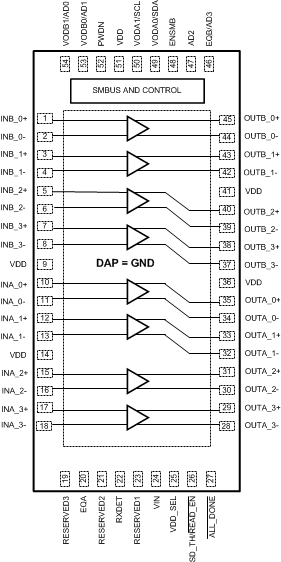
5 Pin Configuration and Functions
54-Pin WQFN
Package NJY
Top View
A.
NOTE:
Above 54-lead WQFN graphic is a TOP VIEW, looking down through the package.Pin Functions(1)
| PIN NAME | PIN NUMBER | I/O, TYPE | DESCRIPTION |
|---|---|---|---|
| DIFFERENTIAL HIGH SPEED I/O | |||
| INB_0+, INB_0- , INB_1+, INB_1-, INB_2+, INB_2-, INB_3+, INB_3- |
1, 2 3, 4 5, 6 7, 8 |
I, CML | Inverting and non-inverting CML differential inputs to the equalizer. On-chip 50 Ω termination resistor connects INB_n+ to VDD and INB_n- to VDD depending on the state of RXDET. See Table 2. AC coupling required on high-speed I/O |
| OUTB_0+, OUTB_0-, OUTB_1+, OUTB_1-, OUTB_2+, OUTB_2-, OUTB_3+, OUTB_3- |
45, 44 43, 42 40, 39 38, 37 |
O, CML | Inverting and non-inverting 50 Ω driver outputs. Compatible with AC coupled CML inputs. AC coupling required on high-speed I/O |
| INA_0+, INA_0- , INA_1+, INA_1-, INA_2+, INA_2-, INA_3+, INA_3- |
10, 11 12, 13 15, 16 17, 18 |
I, CML | Inverting and non-inverting CML differential inputs to the equalizer. On-chip 50 Ω termination resistor connects INA_n+ to VDD and INA_n- to VDD depending on the state of RXDET. See Table 2. AC coupling required on high-speed I/O |
| OUTA_0+, OUTA_0-, OUTA_1+, OUTA_1-, OUTA_2+, OUTA_2-, OUTA_3+, OUTA_3- |
35, 34 33, 32 31, 30 29, 28 |
O, CML | Inverting and non-inverting 50 Ω driver outputs. Compatible with AC coupled CML inputs. AC coupling required on high-speed I/O |
| CONTROL PINS — SHARED (LVCMOS) | |||
| ENSMB | 48 | I, 4-LEVEL, LVCMOS |
System Management Bus (SMBus) Enable Pin Tie 1 kΩ to VDD (2.5 V mode) or VIN (3.3 V mode) = Register Access SMBus Slave Mode FLOAT = Read External EEPROM (SMBus Master Mode) Tie 1 kΩ to GND = Pin Mode |
| ENSMB = 1 (SMBus SLAVE MODE) | |||
| SCL | 50 | I, LVCMOS, O, OPEN Drain |
In SMBus Slave Mode, this pin is the SMBus clock I/O. Clock input or open drain output. External 2 kΩ to 5 kΩ pull-up resistor required as per SMBus interface standards(2) |
| SDA | 49 | I, LVCMOS, O, OPEN Drain |
In both SMBus Modes, this pin is the SMBus data I/O. Data input or open drain output. External 2 kΩ to 5 kΩ pull-up resistor required as per SMBus interface standards(2) |
| AD0-AD3 | 54, 53, 47, 46 | I, LVCMOS | SMBus Slave Address Inputs. In both SMBus Modes, these pins are the user set SMBus slave address inputs. External 1 kΩ pull-up or pull-down recommended. Note: In Pin Mode, AD2 must be tied via external 1 kΩ to GND. |
| RESERVED2 | 21 | I, 4-LEVEL, LVCMOS |
Reserved For applications requiring Signal Detect status register read-back: ● Leave Pin 21 floating. ● Write Reg 0x08[2] = 1 if Pin 21 is floating. Otherwise, tie Pin 21 via external 1 kΩ to GND (External 1 kΩ to VDD (2.5 V mode) or VIN (3.3 V mode) is also acceptable). |
| RESERVED3 | 19 | I, 4-LEVEL, LVCMOS |
Reserved This input may be left floating, tied via 1 kΩ to VDD (2.5 V mode) or VIN (3.3 V mode), or tied via 1 kΩ to GND. |
| ENSMB = Float (SMBus MASTER MODE) | |||
| SCL | 50 | I, LVCMOS, O, OPEN Drain |
Clock output when loading EEPROM configuration, reverting to SMBus clock input when EEPROM load is complete (ALL_DONE = 0). External 2 kΩ to 5 kΩ pull-up resistor required as per SMBus interface standards(2) |
| SDA | 49 | I, LVCMOS, O, OPEN Drain |
In both SMBus Modes, this pin is the SMBus data I/O. Data input or open drain output. External 2 kΩ to 5 kΩ pull-up resistor required as per SMBus interface standards(2) |
| AD0-AD3 | 54, 53, 47, 46 | I, LVCMOS | SMBus Slave Address Inputs. In both SMBus Modes, these pins are the user set SMBus slave address inputs. External 1 kΩ pull-up or pull-down recommended. Note: In Pin Mode, AD2 must be tied via external 1 kΩ to GND. |
| READ_EN | 26 | I, LVCMOS | A logic low on this pin starts the load from the external EEPROM(3). Once EEPROM load is complete (ALL_DONE = 0), this pin functionality remains as READ_EN. It does not revert to an SD_TH input. |
| RESERVED2 | 21 | I, 4-LEVEL, LVCMOS |
Reserved For applications requiring Signal Detect status register read-back: ● Leave Pin 21 floating. ● Write Reg 0x08[2] = 1 if Pin 21 is floating. Otherwise, tie Pin 21 via external 1 kΩ to GND (External 1 kΩ to VDD (2.5 V mode) or VIN (3.3 V mode) is also acceptable). |
| RESERVED3 | 19 | I, 4-LEVEL, LVCMOS |
Reserved This input may be left floating, tied via 1 kΩ to VDD (2.5 V mode) or VIN (3.3 V mode), or tied via 1 kΩ to GND. |
| ENSMB = 0 (PIN MODE) | |||
| EQA EQB |
20 46 |
I, 4-LEVEL, LVCMOS |
EQA and EQB pins control the level of equalization for the A-channels and B-channels, respectively. The pins are defined as EQA and EQB only when ENSMB is de-asserted (low). Each of the four A-channels have the same level unless controlled by the SMBus control registers. Likewise, each of the four B-channels have the same level unless controlled by the SMBus control registers. When the device operates in Slave or Master Mode, the SMBus registers independently control each lane, and the EQB pin is converted to an AD3 input. See Table 4. |
| VODB0 VODB1 |
53 54 |
I, 4-LEVEL, LVCMOS |
VODB[1:0] controls the output amplitude of the B-channels. The pins are defined as VODB[1:0] only when ENSMB is de-asserted (low). Each of the four B-channels have the same level unless controlled by the SMBus control registers. When the device operates in Slave or Master Mode, the SMBus registers provide independent control of each lane, and VODB[1:0] pins are converted to AD0, AD1 inputs. See Table 5. |
| VODA0 VODA1 |
49 50 |
I, 4-LEVEL, LVCMOS |
VODA[1:0] controls the output amplitude of the A-channels. The pins are defined as VODA[1:0] only when ENSMB is de-asserted (low). Each of the four A-channels have the same level unless controlled by the SMBus control registers. When the device operates in Slave or Master Mode, the SMBus registers provide independent control of each lane and the VODA[1:0] pins are converted to SCL and SDA. See Table 5. |
| AD2 | 47 | I, LVCMOS | Reserved in Pin Mode (ENSMB = 0) This input must be tied via external 1 kΩ to GND. |
| SD_TH | 26 | I, 4-LEVEL, LVCMOS |
Controls the internal Signal Detect Status Threshold value when in Pin Mode and SMBus Slave Mode. This pin is to be used for system debugging only, as the signal detect threshold has no impact on the data path. See Table 3 for more information. For final designs, input can be left floating, tied via 1 kΩ to VDD (2.5 V mode) or VIN (3.3 V mode), or tied via 1 kΩ to GND. |
| RESERVED2 | 21 | I, 4-LEVEL, LVCMOS |
Reserved Tie via external 1 kΩ to GND (External 1 kΩ to VDD (2.5 V mode) or VIN (3.3 V mode) is also acceptable). |
| RESERVED3 | 19 | I, 4-LEVEL, LVCMOS |
Reserved This input must be tied via external 1 kΩ to GND. |
| CONTROL PINS — BOTH PIN AND SMBUS MODES (LVCMOS) | |||
| RXDET | 22 | I, 4-LEVEL, LVCMOS |
The RXDET pin controls the RX detection function. Depending on the input level, a 50 Ω or >50 kΩ termination to the power rail is enabled. Keep this input floating for normal PCIe operation. See Table 2. |
| RESERVED1 | 23 | I, 4-LEVEL, LVCMOS |
Reserved This input must be left floating. |
| VDD_SEL | 25 | I, FLOAT | Controls the internal regulator Float = 2.5 V mode Tie to GND = 3.3 V mode See Figure 31. |
| PWDN | 52 | I, LVCMOS | Tie High = Low power - Power Down Tie to GND = Normal Operation See Table 2. |
| ALL_DONE | 27 | O, LVCMOS | Valid Register Load Status Output HIGH = External EEPROM load failed or incomplete LOW = External EEPROM load passed |
| POWER | |||
| VIN | 24 | Power | In 3.3 V mode, feed 3.3 V to VIN In 2.5 V mode, leave floating. |
| VDD | 9, 14, 36, 41, 51 | Power | Power Supply for CML and Analog Pins In 2.5 V mode, connect to 2.5 V In 3.3 V mode, connect 0.1 µF cap to each VDD Pin and GND See Figure 31 for proper power supply decoupling . |
| GND | DAP | Power | Ground pad (DAP - die attach pad). |
(1) LVCMOS inputs without the “Float” conditions must be driven to a logic low or high at all times or operation is not ensured.
Input edge rate for LVCMOS/FLOAT inputs must be faster than 50 ns from 10–90%.
For 3.3 V mode operation, VIN pin input = 3.3 V and the logic "1" or "high" reference for the 4-level input is 3.3 V.
For 2.5 V mode operation, VDD pin output= 2.5 V and the logic "1" or "high" reference for the 4-level input is 2.5 V.
(2) SCL and SDA pins can be tied either to 3.3 V or 2.5 V, regardless of whether the device is operating in 2.5 V mode or 3.3 V mode.
(3) When READ_EN is asserted low, the device attempts to load EEPROM. If EEPROM cannot be loaded successfully, for example due to an invalid or blank hex file, the DS80PCI810 waits indefinitely in an unknown state where SMBus access is not possible. ALL_DONE pin remains high in this situation.