SNLS493A October 2014 – January 2015 DS80PCI810
PRODUCTION DATA.
- 1 Features
- 2 Applications
- 3 Description
- 4 Revision History
- 5 Pin Configuration and Functions
- 6 Specifications
- 7 Detailed Description
- 8 Applications and Implementation
- 9 Power Supply Recommendations
- 10Layout
- 11Device and Documentation Support
- 12Mechanical, Packaging, and Orderable Information
Package Options
Mechanical Data (Package|Pins)
- NJY|54
Thermal pad, mechanical data (Package|Pins)
Orderable Information
9 Power Supply Recommendations
Two approaches are recommended to ensure that the DS80PCI810 is provided with an adequate power supply. First, the supply (VDD) and ground (GND) pins should be connected to power planes routed on adjacent layers of the printed circuit board. The layer thickness of the dielectric should be minimized so that the VDD and GND planes create a low inductance supply with distributed capacitance. Second, careful attention to supply bypassing through the proper use of bypass capacitors is required. A 0.1 μF bypass capacitor should be connected to each VDD pin such that the capacitor is placed as close as possible to the DS80PCI810. Smaller body size capacitors can help facilitate proper component placement. Additionally, capacitor with capacitance in the range of 1 μF to 10 μF should be incorporated in the power supply bypassing design as well. These capacitors can be either tantalum or an ultra-low ESR ceramic.
The DS80PCI810 has an optional internal voltage regulator to provide the 2.5 V supply to the device. In 3.3 V mode operation, the VIN pin = 3.3 V is used to supply power to the device. The internal regulator then provides the 2.5 V to the VDD pins of the device, and a 0.1 μF cap is needed at each of the five VDD pins for power supply de-coupling (total capacitance should equal 0.5 μF). The VDD_SEL pin must be tied to GND to enable the internal regulator. In 2.5 V mode operation, the VIN pin should be left open and 2.5 V supply must be applied to the five VDD pins to power the device. The VDD_SEL pin must be left open (no connect) to disable the internal regulator.
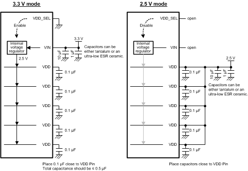 Figure 31. 3.3 V or 2.5 V Supply Connection Diagram