SNLS416D June 2012 – January 2015 DS90UB927Q-Q1
PRODUCTION DATA.
- 1 Features
- 2 Applications
- 3 Description
- 4 Revision History
- 5 Pin Configuration and Functions
-
6 Specifications
- 6.1 Absolute Maximum Ratings
- 6.2 ESD Ratings
- 6.3 Recommended Operating Conditions
- 6.4 Thermal Information
- 6.5 DC Electrical Characteristics
- 6.6 AC Electrical Characteristics
- 6.7 Electrical Characteristics: DC and AC Serial Control Bus
- 6.8 Timing Requirements for the Serial Control Bus
- 6.9 Timing Requirements - DC and AC Serial Control Bus Characteristics
- 6.10 Typical Characteristics
-
7 Detailed Description
- 7.1 Overview
- 7.2 Functional Block Diagram
- 7.3
Feature Description
- 7.3.1 High-Speed Forward Channel Data Transfer
- 7.3.2 Low-Speed Back Channel Data Transfer
- 7.3.3 Common Mode Filter Pin (CMF)
- 7.3.4 Video Control Signals
- 7.3.5 EMI Reduction Features
- 7.3.6 Built-In Self Test (BIST)
- 7.3.7 Forward Channel and Back Channel Error Checking
- 7.3.8 Internal Pattern Generation
- 7.3.9 Remote Auto Power-Down Mode
- 7.3.10 Input RxCLKIN Loss Detect
- 7.3.11 Serial Link Fault Detect
- 7.3.12 Interrupt Pin (INTB)
- 7.3.13 General-Purpose I/O
- 7.3.14 I2S Audio Interface
- 7.3.15 Additional Features
- 7.4 Device Functional Modes
- 7.5 Programming
- 7.6 Register Maps
- 8 Application and Implementation
- 9 Power Supply Recommendations
- 10Layout
- 11Device and Documentation Support
- 12Mechanical, Packaging, and Orderable Information
Package Options
Refer to the PDF data sheet for device specific package drawings
Mechanical Data (Package|Pins)
- RTA|40
Thermal pad, mechanical data (Package|Pins)
- RTA|40
Orderable Information
8 Application and Implementation
NOTE
Information in the following applications sections is not part of the TI component specification, and TI does not warrant its accuracy or completeness. TI’s customers are responsible for determining suitability of components for their purposes. Customers should validate and test their design implementation to confirm system functionality.
8.1 Application Information
The DS90UB927Q-Q1, in conjunction with the DS90UB928Q-Q1 or DS90UB926Q-Q1, is intended for interface between a host (graphics processor) and a display, supporting 24-bit color depth (RGB888) and high definition (720p) digital video format. It can receive an 8-bit RGB stream with a pixel clock rate up to 85 MHz together with three control bits (VS, HS and DE) and four I2S audio streams.
8.2 Typical Application
Figure 29 shows a typical application of the DS90UB927Q-Q1 serializer for an 85-MHz 24-bit Color Display Application. The 5 LVDS input pairs require external 100Ω terminations. The CML outputs must have an external 0.1-µF AC coupling capacitor on the high speed serial lines. The serializer has internal CML termination on its high speed outputs.
Bypass capacitors should be placed near the power supply pins. At a minimum, four (4) 4.7-µF capacitors should be used for local device bypassing. Ferrite beads are placed on the two sets of supply pins (VDD33 and VDDIO) for effective noise suppression. The interface to the graphics source is LVDS. The VDDIO pins may be connected to 3.3 V or 1.8 V. A capacitor and resistor are placed on the PDB pin to delay the enabling of the device until power is stable.
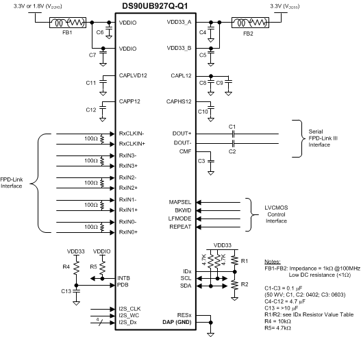 Figure 29. Color Display Typical Connection Diagram
8.2.1 Design Requirements
For the typical design application, use the following as input parameters.
Table 6. Design Parameters
| DESIGN PARAMETER | EXAMPLE VALUE |
|---|---|
| VDDIO | 1.8 V or 3.3 V |
| VDD33 | 3.3 V |
| AC Coupling Capacitor for DOUT± | 100 nF |
| PCLK Frequency | 85 MHz |
8.2.2 Detailed Design Procedure
Figure 29 shows a typical application of the DS90UB927Q-Q1 serializer for an 85-MHz 24-bit Color Display Application. The CML outputs must have an external 0.1-μF AC coupling capacitor on the high speed serial lines. Bypass capacitors are placed near the power supply pins. At a minimum, six 4.7-μF capacitors and two additional 1-μF capacitors should be used for local device bypassing. Ferrite beads are placed on the two VDDs (VDD33 and VDDIO) for effective noise suppression. An RC delay is placed on the PDB signal to delay the enabling of the device until power is stable.
8.2.3 Application Curves
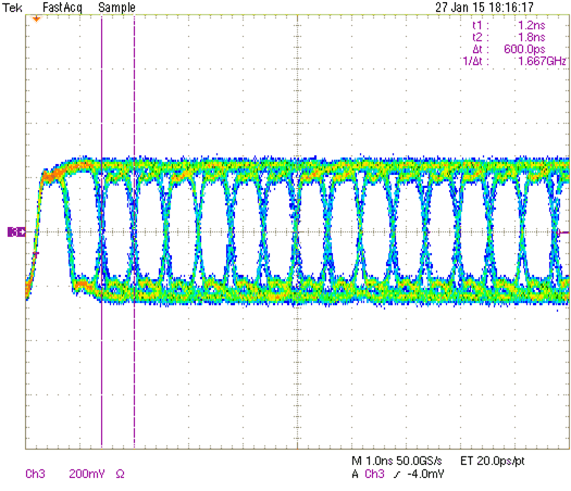 Figure 30. Serializer Output Stream with 48-MHz Input Clock
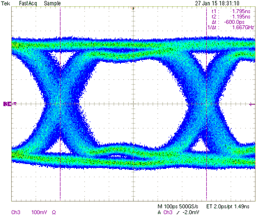 Figure 31. Serializer Eye with 48-MHz Input Clock
8.3 System Examples
 Figure 32. Color Display Application Diagram
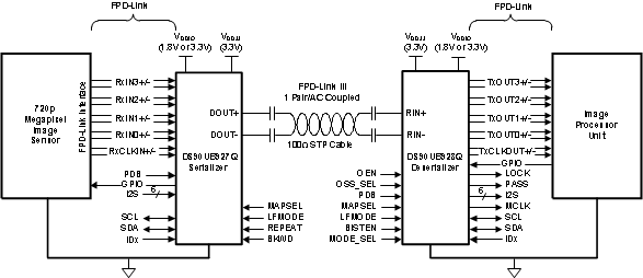 Figure 33. Megapixel Camera Application Diagram