SNLS416D June 2012 – January 2015 DS90UB927Q-Q1
PRODUCTION DATA.
- 1 Features
- 2 Applications
- 3 Description
- 4 Revision History
- 5 Pin Configuration and Functions
-
6 Specifications
- 6.1 Absolute Maximum Ratings
- 6.2 ESD Ratings
- 6.3 Recommended Operating Conditions
- 6.4 Thermal Information
- 6.5 DC Electrical Characteristics
- 6.6 AC Electrical Characteristics
- 6.7 Electrical Characteristics: DC and AC Serial Control Bus
- 6.8 Timing Requirements for the Serial Control Bus
- 6.9 Timing Requirements - DC and AC Serial Control Bus Characteristics
- 6.10 Typical Characteristics
-
7 Detailed Description
- 7.1 Overview
- 7.2 Functional Block Diagram
- 7.3
Feature Description
- 7.3.1 High-Speed Forward Channel Data Transfer
- 7.3.2 Low-Speed Back Channel Data Transfer
- 7.3.3 Common Mode Filter Pin (CMF)
- 7.3.4 Video Control Signals
- 7.3.5 EMI Reduction Features
- 7.3.6 Built-In Self Test (BIST)
- 7.3.7 Forward Channel and Back Channel Error Checking
- 7.3.8 Internal Pattern Generation
- 7.3.9 Remote Auto Power-Down Mode
- 7.3.10 Input RxCLKIN Loss Detect
- 7.3.11 Serial Link Fault Detect
- 7.3.12 Interrupt Pin (INTB)
- 7.3.13 General-Purpose I/O
- 7.3.14 I2S Audio Interface
- 7.3.15 Additional Features
- 7.4 Device Functional Modes
- 7.5 Programming
- 7.6 Register Maps
- 8 Application and Implementation
- 9 Power Supply Recommendations
- 10Layout
- 11Device and Documentation Support
- 12Mechanical, Packaging, and Orderable Information
Package Options
Refer to the PDF data sheet for device specific package drawings
Mechanical Data (Package|Pins)
- RTA|40
Thermal pad, mechanical data (Package|Pins)
- RTA|40
Orderable Information
5 Pin Configuration and Functions
RTA Package
40-Pin WQFN With Exposed Thermal Pad
Top View
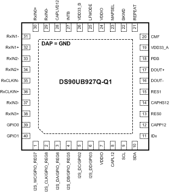
Pin Functions
| PIN | I/O | DESCRIPTION | |
|---|---|---|---|
| NAME | NO. | ||
| FPD-LINK INPUT INTERFACE | |||
| RxCLKIN- | 35 | I, LVDS | Inverting LVDS Clock Input The pair requires external 100-Ω differential termination for standard LVDS levels |
| RxCLKIN+ | 36 | I, LVDS | True LVDS Clock Input The pair requires external 100-Ω differential termination for standard LVDS levels |
| RxIN[3:0]- | 37, 33, 31, 29 |
I, LVDS | Inverting LVDS Data Inputs Each pair requires external 100-Ω differential termination for standard LVDS levels |
| RxIN[3:0]+ | 38, 34, 32, 30 |
I, LVDS | True LVDS Data Inputs Each pair requires external 100-Ω differential termination for standard LVDS levels |
| LVCMOS PARALLEL INTERFACE | |||
| BKWD | 22 | I, LVCMOS with pulldown |
Backward Compatible Mode Select BKWD = 0, interfacing to DS90UH926/8Q-Q1 (Default) BKWD = 1, interfacing to DS90UR906/8Q-Q1, DS90UR916Q Requires a 10-kΩ pullup if set HIGH |
| GPIO[1:0] | 40, 39 | I/O, LVCMOS with pulldown |
General Purpose I/O See Table 1 |
| I2S_DA I2S_DB I2S_DC I2S_DD |
3 4 5 6 |
I, LVCMOS with pulldown |
Digital Audio Interface I2S Data Inputs Shared with GPIO_REG6, GPIO_REG5, GPIO2, GPIO3 |
| I2S_WC I2S_CLK |
1 2 |
I, LVCMOS with pulldown |
Digital Audio Interface I2S Word Clock and I2S Bit Clock Inputs Shared with GPIO_REG7 and GPIO_REG8 (Table 3) |
| LFMODE | 25 | I, LVCMOS with pulldown |
Low Frequency Mode Select LFMODE = 0, 15 MHz ≤ RxCLKIN ≤ 85 MHz (Default) LFMODE = 1, 5 MHz ≤ RxCLKIN < 15 MHz Requires a 10-kΩ pullup if set HIGH |
| MAPSEL | 23 | I, LVCMOS with pulldown |
FPD-Link Input Map Select MAPSEL = 0, LSBs on RxIN3± (Default) MAPSEL = 1, MSBs on RxIN3± See Figure 19 and Figure 20 Requires a 10-kΩ pullup if set HIGH |
| REPEAT | 21 | I, LVCMOS with pulldown |
Repeater Mode Select REPEAT = 0, Repeater Mode disabled (Default) REPEAT = 1, Repeater Mode enabled Requires a 10-kΩ pullup if set HIGH |
| OPTIONAL PARALLEL INTERFACE | |||
| GPIO[3:2] | 6, 5 | I/O, LVCMOS with pulldown |
General Purpose I/O Shared with I2S_DD and I2S_DC (See Table 1) |
| GPIO_REG [8:5] |
2, 1, 3, 4 | I/O, LVCMOS with pulldown |
Register-Only General Purpose I/O Shared with I2S_CLK, I2S_WC, I2S_DA, I2S_DB (See Table 2) |
| CONTROL AND CONFIGURATION | |||
| IDx | 11 | I, Analog | I2C Address Select External pullup to VDD33 is required under all conditions. DO NOT FLOAT. Connect to external pullup to VDD33 and pulldown to GND to create a voltage divider. See Figure 25 and Table 4 |
| PDB | 18 | I, LVCMOS with pulldown |
Power-down Mode Input Pin Must be driven or pulled up to VDD33. Refer to Power Supply Recommendations. PDB = H, device is enabled (normal operation) PDB = L, device is powered down. When the device is in the powered down state, the Driver Outputs are both HIGH, the PLL is shutdown, and IDD is minimized. Control Registers are RESET. |
| SCL | 9 | I/O, LVCMOS Open Drain |
I2C Clock Input / Output Interface Must have an external pullup to VDD33. DO NOT FLOAT. Recommended pullup: 4.7 kΩ. |
| SDA | 10 | I/O, LVCMOS Open Drain |
I2C Data Input / Output Interface Must have an external pullup to VDD33. DO NOT FLOAT. Recommended pullup: 4.7 kΩ. |
| STATUS | |||
| INTB | 27 | O, LVCMOS Open Drain |
Interrupt INTB = H, normal INTB = L, Interrupt request Recommended pullup: 4.7 kΩ to VDDIO. DO NOT FLOAT. |
| FPD-LINK III SERIAL INTERFACE | |||
| CMF | 20 | Analog | Common Mode Filter. Connect 0.1 µF to GND (required) |
| DOUT- | 16 | I/O, LVDS | Inverting Output The output must be AC-coupled with a 0.1-µF capacitor. |
| DOUT+ | 17 | I/O, LVDS | True Output The output must be AC-coupled with a 0.1-µF capacitor. |
| POWER(1) AND GROUND | |||
| GND | DAP | Ground | Large metal contact at the bottom center of the device package Connect to the ground plane (GND) with at least 9 vias. |
| VDD33_A VDD33_B |
19 26 |
Power | Power to on-chip regulator 3.0 V - 3.6 V. Each pin requires a 4.7-µF capacitor to GND |
| VDDIO | 7, 24 | Power | LVCMOS I/O Power 1.8 V ±5% OR 3.0 V - 3.6 V. Each pin requires 4.7-µF capacitor to GND |
| REGULATOR CAPACITOR | |||
| CAPL12 | 8 | CAP | Decoupling capacitor connection for on-chip regulator Requires two 4.7-µF decoupling capacitors to GND |
| CAPP12 CAPHS12 CAPLVD12 |
12 14 28 |
CAP | Decoupling capacitor connection for on-chip regulator Each requires a 4.7-µF decoupling capacitor to GND. |
| OTHER | |||
| RES[1:0] | 15, 13 | GND | Reserved Connect to GND. |
(1) The VDD (VDD33 and VDDIO) supply ramp should be faster than 1.5 ms with a monotonic rise.