SNLS313I September 2009 – October 2019 DS90UR905Q-Q1 , DS90UR906Q-Q1
PRODUCTION DATA.
- 1 Features
- 2 Applications
- 3 Description
- 4 Revision History
- 5 Description (continued)
- 6 Pin Configuration and Functions
-
7 Specifications
- 7.1 Absolute Maximum Ratings
- 7.2 ESD Ratings
- 7.3 Recommended Operating Conditions
- 7.4 Thermal Information
- 7.5 Serializer DC Electrical Characteristics
- 7.6 Deserializer DC Electrical Characteristics
- 7.7 DC and AC Serial Control Bus Characteristics
- 7.8 Timing Requirements for DC and AC Serial Control Bus
- 7.9 Timing Requirements for Serializer PCLK
- 7.10 Timing Requirements for Serial Control Bus
- 7.11 Switching Characteristics: Serializer
- 7.12 Switching Characteristics: Deserializer
- 7.13 Typical Characteristics
-
8 Detailed Description
- 8.1 Overview
- 8.2 Functional Block Diagrams
- 8.3
Feature Description
- 8.3.1 Data Transfer
- 8.3.2 Video Control Signal Filter — Serializer and Deserializer
- 8.3.3 Serializer Functional Description
- 8.3.4
Deserializer Functional Description
- 8.3.4.1 Signal Quality Enhancers
- 8.3.4.2 EMI Reduction Features
- 8.3.4.3 Power-Saving Features
- 8.3.4.4 Deserializer CLOCK-DATA RECOVERY STATUS FLAG (LOCK) and OUTPUT STATE SELECT (OSS_SEL)
- 8.3.4.5 Deserializer Oscillator Output (Optional)
- 8.3.4.6 Deserializer OP_LOW (Optional)
- 8.3.4.7 Deserializer Pixel Clock Edge Select (RFB)
- 8.3.4.8 Deserializer Control Signal Filter (Optional)
- 8.3.4.9 Deserializer Low Frequency Optimization (LF_Mode)
- 8.3.4.10 Deserializer Map Select
- 8.3.4.11 Deserializer Strap Input Pins
- 8.3.4.12 Optional Serial Bus Control
- 8.3.4.13 Optional BIST Mode
- 8.3.5 Built-In Self Test (BIST)
- 8.3.6 Optional Serial Bus Control
- 8.4 Device Functional Modes
- 8.5 Register Maps
- 9 Application and Implementation
- 10Power Supply Recommendations
- 11Layout
- 12Device and Documentation Support
- 13Mechanical, Packaging, and Orderable Information
Package Options
Mechanical Data (Package|Pins)
- RHS|48
Thermal pad, mechanical data (Package|Pins)
- RHS|48
Orderable Information
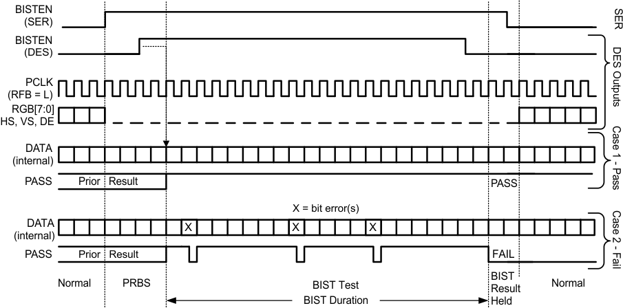
8.3.5.2 BER Calculations
It is possible to calculate the approximate Bit Error Rate (BER). The following is required:
- Pixel Clock Frequency (MHz)
- BIST Duration (seconds)
- BIST test Result (PASS)
The BER is less than or equal to one over the product of 24 times the PCLK rate times the test duration. If we assume a 65-MHz PCLK, a 10 minute (600 seconds) test, and a PASS, the BERT is ≤ 1.07 × 10E-12.
The BIST mode runs a check on the data payload bits. The LOCK pin also provides a link status. It the recovery of the C0 and C1 bits does not reconstruct the expected clock signal, the LOCK pin will switch Low. The combination of the LOCK and At-Speed BIST PASS pin provides a powerful tool for system evaluation and performance monitoring.
 Figure 33. BIST Waveforms