SNLS313I September 2009 – October 2019 DS90UR905Q-Q1 , DS90UR906Q-Q1
PRODUCTION DATA.
- 1 Features
- 2 Applications
- 3 Description
- 4 Revision History
- 5 Description (continued)
- 6 Pin Configuration and Functions
-
7 Specifications
- 7.1 Absolute Maximum Ratings
- 7.2 ESD Ratings
- 7.3 Recommended Operating Conditions
- 7.4 Thermal Information
- 7.5 Serializer DC Electrical Characteristics
- 7.6 Deserializer DC Electrical Characteristics
- 7.7 DC and AC Serial Control Bus Characteristics
- 7.8 Timing Requirements for DC and AC Serial Control Bus
- 7.9 Timing Requirements for Serializer PCLK
- 7.10 Timing Requirements for Serial Control Bus
- 7.11 Switching Characteristics: Serializer
- 7.12 Switching Characteristics: Deserializer
- 7.13 Typical Characteristics
-
8 Detailed Description
- 8.1 Overview
- 8.2 Functional Block Diagrams
- 8.3
Feature Description
- 8.3.1 Data Transfer
- 8.3.2 Video Control Signal Filter — Serializer and Deserializer
- 8.3.3 Serializer Functional Description
- 8.3.4
Deserializer Functional Description
- 8.3.4.1 Signal Quality Enhancers
- 8.3.4.2 EMI Reduction Features
- 8.3.4.3 Power-Saving Features
- 8.3.4.4 Deserializer CLOCK-DATA RECOVERY STATUS FLAG (LOCK) and OUTPUT STATE SELECT (OSS_SEL)
- 8.3.4.5 Deserializer Oscillator Output (Optional)
- 8.3.4.6 Deserializer OP_LOW (Optional)
- 8.3.4.7 Deserializer Pixel Clock Edge Select (RFB)
- 8.3.4.8 Deserializer Control Signal Filter (Optional)
- 8.3.4.9 Deserializer Low Frequency Optimization (LF_Mode)
- 8.3.4.10 Deserializer Map Select
- 8.3.4.11 Deserializer Strap Input Pins
- 8.3.4.12 Optional Serial Bus Control
- 8.3.4.13 Optional BIST Mode
- 8.3.5 Built-In Self Test (BIST)
- 8.3.6 Optional Serial Bus Control
- 8.4 Device Functional Modes
- 8.5 Register Maps
- 9 Application and Implementation
- 10Power Supply Recommendations
- 11Layout
- 12Device and Documentation Support
- 13Mechanical, Packaging, and Orderable Information
Package Options
Mechanical Data (Package|Pins)
- RHS|48
Thermal pad, mechanical data (Package|Pins)
- RHS|48
Orderable Information
8.3.6 Optional Serial Bus Control
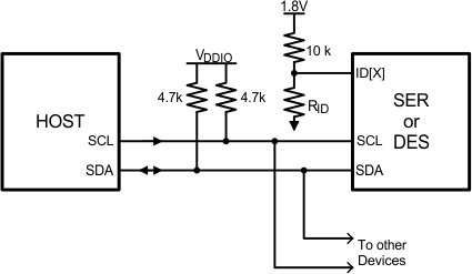
The serializer and deserializer may also be configured by the use of a serial control bus that is I2C protocol compatible. By default, the I2C reg_0x00'h is set to 00'h and all configuration is set by control/strap pins. A write of 01'h to reg_0x00'h will enable or allow configuration by registers; this will override the control/strap pins. Multiple devices may share the serial control bus since multiple addresses are supported (see Figure 34).
The serial bus is comprised of three pins. The SCL is a serial bus clock Input. The SDA is the serial bus data input/output signal. Both SCL and SDA signals require an external pullup resistor to VDDIO. For most applications a 4.7-k pullup resistor to VDDIO may be used. The resistor value may be adjusted for capacitive loading and data rate requirements. The signals are either pulled High, or driven Low.
 Figure 34. Serial Control Bus Connection
 The third pin is the ID[X] pin. This pin sets one of four possible device addresses. Two different connections are possible. The pin may be pulled to VDD (1.8V, NOT VDDIO) with a 10 kΩ resistor; or a 10-kΩ pullup resistor (to VDD1.8V, NOT VDDIO) and a pulldown resistor of the recommended value to set other three possible addresses may be used. See Table 10 for the serializer and Table 11 for the deserializer. Do not tie ID[x] directly to VSS.
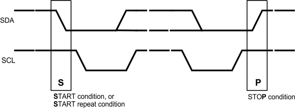
The Serial Bus protocol is controlled by START, START-Repeated, and STOP phases. A START occurs when SCL transitions Low while SDA is High. A STOP occurs when SDA transition High while SCL is also HIGH (see Figure 35).
 Figure 35. START and STOP Conditions
 To communicate with a remote device, the host controller (master) sends the slave address and listens for a response from the slave. This response is referred to as an acknowledge bit (ACK). If a slave on the bus is addressed correctly, it Acknowledges (ACKs) the master by driving the SDA bus low. If the address doesn't match a device's slave address, it Not-acknowledges (NACKs) the master by letting SDA be pulled High. ACKs also occur on the bus when data is being transmitted. When the master is writing data, the slave ACKs after every data byte is successfully received. When the master is reading data, the master ACKs after every data byte is received to let the slave know it wants to receive another data byte. When the master wants to stop reading, it NACKs after the last data byte and creates a stop condition on the bus. All communication on the bus begins with either a Start condition or a Repeated Start condition. All communication on the bus ends with a Stop condition. A READ is shown in Figure 36 and a WRITE is shown in Figure 37.
NOTE
During initial power-up, a delay of 10 ms will be required before the I2C will respond.
If the Serial Bus is not required, the three pins may be left open (NC).
Table 10. ID[x] Resistor Value – DS90UR905Q-Q1 Serializer
| RESISTOR
RID(1) kΩ (5% TOL) |
ADDRESS
7'b |
ADDRESS
8'b 0 APPENDED (WRITE) |
|---|---|---|
| 0.47 | 7b' 110 1001 (h'69) | 8b' 1101 0010 (h'D2) |
| 2.7 | 7b' 110 1010 (h'6A) | 8b' 1101 0100 (h'D4) |
| 8.2 | 7b' 110 1011 (h'6B) | 8b' 1101 0110 (h'D6) |
| Open | 7b' 110 1110 (h'6E) | 8b' 1101 1100 (h'DC) |
Table 11. ID[x] Resistor Value – DS90UR906Q-Q1 Deserializer
| RESISTOR
RID(1) kΩ (5% TOL) |
ADDRESS
7'b |
ADDRESS
8'b 0 APPENDED (WRITE) |
|---|---|---|
| 0.47 | 7b' 111 0001 (h'71) | 8b' 1110 0010 (h'E2) |
| 2.7 | 7b' 111 0010 (h'72) | 8b' 1110 0100 (h'E4) |
| 8.2 | 7b' 111 0011 (h'73) | 8b' 1110 0110 (h'E6) |
| Open | 7b' 111 0110 (h'76) | 8b' 1110 1100 (h'EC) |
 Figure 36. Serial Control Bus — READ
  Figure 37. Serial Control Bus — WRITE