SNLS313I September 2009 – October 2019 DS90UR905Q-Q1 , DS90UR906Q-Q1
PRODUCTION DATA.
- 1 Features
- 2 Applications
- 3 Description
- 4 Revision History
- 5 Description (continued)
- 6 Pin Configuration and Functions
-
7 Specifications
- 7.1 Absolute Maximum Ratings
- 7.2 ESD Ratings
- 7.3 Recommended Operating Conditions
- 7.4 Thermal Information
- 7.5 Serializer DC Electrical Characteristics
- 7.6 Deserializer DC Electrical Characteristics
- 7.7 DC and AC Serial Control Bus Characteristics
- 7.8 Timing Requirements for DC and AC Serial Control Bus
- 7.9 Timing Requirements for Serializer PCLK
- 7.10 Timing Requirements for Serial Control Bus
- 7.11 Switching Characteristics: Serializer
- 7.12 Switching Characteristics: Deserializer
- 7.13 Typical Characteristics
-
8 Detailed Description
- 8.1 Overview
- 8.2 Functional Block Diagrams
- 8.3
Feature Description
- 8.3.1 Data Transfer
- 8.3.2 Video Control Signal Filter — Serializer and Deserializer
- 8.3.3 Serializer Functional Description
- 8.3.4
Deserializer Functional Description
- 8.3.4.1 Signal Quality Enhancers
- 8.3.4.2 EMI Reduction Features
- 8.3.4.3 Power-Saving Features
- 8.3.4.4 Deserializer CLOCK-DATA RECOVERY STATUS FLAG (LOCK) and OUTPUT STATE SELECT (OSS_SEL)
- 8.3.4.5 Deserializer Oscillator Output (Optional)
- 8.3.4.6 Deserializer OP_LOW (Optional)
- 8.3.4.7 Deserializer Pixel Clock Edge Select (RFB)
- 8.3.4.8 Deserializer Control Signal Filter (Optional)
- 8.3.4.9 Deserializer Low Frequency Optimization (LF_Mode)
- 8.3.4.10 Deserializer Map Select
- 8.3.4.11 Deserializer Strap Input Pins
- 8.3.4.12 Optional Serial Bus Control
- 8.3.4.13 Optional BIST Mode
- 8.3.5 Built-In Self Test (BIST)
- 8.3.6 Optional Serial Bus Control
- 8.4 Device Functional Modes
- 8.5 Register Maps
- 9 Application and Implementation
- 10Power Supply Recommendations
- 11Layout
- 12Device and Documentation Support
- 13Mechanical, Packaging, and Orderable Information
Package Options
Mechanical Data (Package|Pins)
- RHS|48
Thermal pad, mechanical data (Package|Pins)
- RHS|48
Orderable Information
9.2.2 DS90UR906Q-Q1 Typical Connection
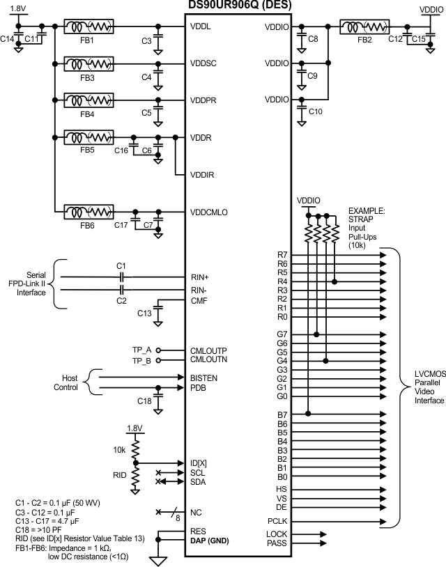
Figure 41 shows a typical application of the DS90UR906Q-Q1 deserializer in Pin/STRAP control mode for a 65-MHz 24-bit Color Display Application. The LVDS inputs utilize 100-nF coupling capacitors to the line and the receiver provides internal termination. Bypass capacitors are placed near the power supply pins. At a minimum, seven 0.1-µF capacitors and two 4.7-µF capacitors should be used for local device bypassing. System GPO (General-Purpose Output) signals control the PDB and the BISTEN pins. In this application the RRFB pin is tied Low to strobe the data on the falling edge of the PCLK.
Since the device in the Pin/STRAP mode, four 10-kΩ pullup resistors are used on the parallel output bus to select the desired device features. CONFIG[1:0] is set to 01'b for Normal Mode and Control Signal Filter ON, this is accomplished with the STRAP pullup on B7. The receiver input equalizer is also enabled and set to provide 7.5 dB of gain, this is accomplished with EQ[3:0] set to 1001'b with STRAP pullups on G4 and G7. To reduce parallel bus EMI, the SSCG feature is enabled and set to 30 kHz and ±1% with SSC[3:0] set to 0010'b and a STRAP pullup on R4. The desired features are set with the use of the four pullup resistors.
The interface to the target display is with 3.3V LVCMOS levels, thus the VDDIO pin is connected to the 3.3 V rail. The optional Serial Bus Control is not used in this example, thus the SCL, SDA and ID[x] pins are left open. A delay cap is placed on the PDB signal to delay the enabling of the device until power is stable.
 Figure 41. DS90UR906Q-Q1 Typical Connection Diagram — Pin Control