SNLS321C May 2010 – May 2016 DS92LV2421 , DS92LV2422
PRODUCTION DATA.
- 1 Features
- 2 Applications
- 3 Description
- 4 Revision History
- 5 Pin Configuration and Functions
-
6 Specifications
- 6.1 Absolute Maximum Ratings
- 6.2 ESD Ratings
- 6.3 Recommended Operating Conditions
- 6.4 Thermal Information
- 6.5 Electrical Characteristics - Serializer DC
- 6.6 Electrical Characteristics - Deserializer DC
- 6.7 Electrical Characteristics - DC and AC Serial Control Bus
- 6.8 Timing Requirements - DC and AC Serial Control Bus
- 6.9 Timing Requirements - Serializer for CLKIN
- 6.10 Timing Requirements - Serial Control Bus
- 6.11 Switching Characteristics - Serializer
- 6.12 Switching Characteristics - Deserializer
- 6.13 Typical Characteristics
-
7 Detailed Description
- 7.1 Overview
- 7.2 Functional Block Diagrams
- 7.3
Feature Description
- 7.3.1 Data Transfer
- 7.3.2 Video Control Signal Filter - Serializer and Deserializer
- 7.3.3 Serializer Functional Description
- 7.3.4
Deserializer Functional Description
- 7.3.4.1 Signal Quality Enhancers
- 7.3.4.2 EMI Reduction Features
- 7.3.4.3 Deserializer Clock-Data Recovery Status Flag (LOCK) And Output State Select (OSS_SEL)
- 7.3.4.4 Deserializer Oscillator Output (Optional)
- 7.3.4.5 Deserializer OP_LOW (Optional)
- 7.3.4.6 Deserializer Clock Edge Select (RFB)
- 7.3.4.7 Deserializer Control Signal Filter (Optional)
- 7.3.4.8 Deserializer Low Frequency Optimization (LF_Mode)
- 7.3.4.9 Deserializer Map Select
- 7.3.4.10 Deserializer Strap Input Pins
- 7.3.4.11 Optional Serial Bus Control
- 7.3.4.12 Optional BIST Mode
- 7.3.5 Built-In Self Test (BIST)
- 7.3.6 Optional Serial Bus Control
- 7.4 Device Functional Modes
- 7.5 Register Maps
- 8 Application and Implementation
- 9 Power Supply Recommendations
- 10Layout
- 11Device and Documentation Support
- 12Mechanical, Packaging, and Orderable Information
Package Options
Mechanical Data (Package|Pins)
- RHS|48
Thermal pad, mechanical data (Package|Pins)
- RHS|48
Orderable Information
8 Application and Implementation
NOTE
Information in the following applications sections is not part of the TI component specification, and TI does not warrant its accuracy or completeness. TI’s customers are responsible for determining suitability of components for their purposes. Customers should validate and test their design implementation to confirm system functionality.
8.1 Application Information
8.1.1 Display Application
The DS92LV242x chipset is intended for interface between a host (graphics processor) and a display. It supports a 24-bit color depth (RGB888) and up to 1024 x 768 display formats. In a RGB888 application, 24 color bits (D[23:0]), Pixel Clock (CLKIN), and three control bits (C1, C2, C3) are supported across the serial link with CLKIN rates from 10 to 75 MHz. The chipset may also be used in 18-bit color applications. In this application, three to six general-purpose signals may also be sent from host to display.
The deserializer is expected to be placed close to its target device. The interconnect between the deserializer and the target device is typically in the 1 to 3 inch separation range. The input capacitance of the target device is expected to be in the 5 pF to 10 pF range. Take care of the CLKOUT output trace, as this signal is edge sensitive and strobes the data. It is also assumed that the fanout of the deserializer is one. If additional loads need to be driven, a logic buffer or mux device is recommended.
8.1.2 Live Link Insertion
The serializer and deserializer devices support live pluggable applications. The automatic receiver lock to random data plug and go hot insertion capability allows the DS92LV2422 to attain lock to the active data stream during a live insertion event.
8.1.3 Alternate Color / Data Mapping
Color Mapped Data Pin names are provided to specify a recommended mapping for 24-bit color applications. Seven [7] is assumed to be the MSB, and Zero [0] is assumed to be the LSB. While this is recommended, it is not required. When connecting to earlier generations of FPD-Link II serializer and deserializer devices, a color mapping review is recommended to ensure the correct connectivity is obtained. Table 17 provides examples for interfacing to 18-bit applications with or without the video control signals embedded. The DS92LV2422 deserializer provides additional flexibility with the MAP_SEL feature as well.
Table 17. Alternate Color and Data Mapping
| 18-BIT RGB | 18-BIT RGB | 24-BIT RGB | 2421 PIN NAME | 2422 PIN NAME | 24-BIT RGB | 18-BIT RGB | 18-BIT RGB |
|---|---|---|---|---|---|---|---|
| LSB R0 | GP0 | R0 | DI0 | DO0 | R0 | GP0 | LSB R0 |
| R1 | GP1 | R1 | DI1 | DO1 | R1 | GP1 | R1 |
| R2 | R0 | R2 | DI2 | DO2 | R2 | R0 | R2 |
| R3 | R1 | R3 | DI3 | DO3 | R3 | R1 | R3 |
| R4 | R2 | R4 | DI4 | DO4 | R4 | R2 | R4 |
| MSB R5 | R3 | R5 | DI5 | DO5 | R5 | R3 | MSB R5 |
| LSB G0 | R4 | R6 | DI6 | DO6 | R6 | R4 | LSB G0 |
| G1 | R5 | R7 | DI7 | DO7 | R7 | R5 | G1 |
| G2 | GP2 | G0 | DI8 | DO8 | G0 | GP2 | G2 |
| G3 | GP3 | G1 | DI9 | DO9 | G1 | GP3 | G3 |
| G4 | G0 | G2 | DI10 | DO10 | G2 | G0 | G4 |
| MSB G5 | G1 | G3 | DI11 | DO11 | G3 | G1 | MSB G5 |
| LSB B0 | G2 | G4 | DI12 | DO12 | G4 | G2 | LSB0 |
| B1 | G3 | G5 | DI13 | DO13 | G5 | G3 | B1 |
| B2 | G4 | G6 | DI14 | DO14 | G6 | G4 | B2 |
| B3 | G5 | G7 | DI15 | DO15 | G7 | G5 | B3 |
| B4 | GP4 | B0 | DI16 | DO16 | B0 | GP4 | B4 |
| MSB B5 | GP5 | B1 | DI17 | DO17 | B1 | GP5 | MSB B5 |
| HS | B0 | B2 | DI18 | DO18 | B2 | B0 | HS |
| VS | B1 | B3 | DI19 | DO19 | B3 | B1 | VS |
| DE | B2 | B4 | DI20 | DO20 | B4 | B2 | DE |
| GP0 | B3 | B5 | DI21 | DO21 | B5 | B3 | GP0 |
| GP1 | B4 | B6 | DI22 | DO22 | B6 | B4 | GP1 |
| GP2 | B5 | B7 | DI23 | DO23 | B7 | B5 | GP2 |
| GND | HS | HS | CI1 | CO1 | HS | HS | GND |
| GND | VS | VS | CI2 | CO2 | VS | VS | GND |
| GND | DE | DE | CI3 | CO3 | DE | DE | GND |
| Scenario 3(3) | Scenario 2(2) | Scenario 1(1) | 2421 Pin Name | 2422 Pin Name | Scenario 1(1) | Scenario 2(2) | Scenario 3(3) |
8.2 Typical Applications
8.2.1 DS92LV2421 Typical Connection
Figure 38 shows a typical application of the DS92LV2421 serializer in pin control mode for a 24-bit application. The LVDS outputs require 100-nF AC-coupling capacitors to the line. The line driver includes internal termination. Bypass capacitors are placed near the power supply pins. At a minimum, four 0.1-µF capacitors and a 4.7-µF capacitor must be used for local device bypassing. System GPO (General Purpose Output) signals control the PDB and BISTEN pins. In this application, the RFB pin is tied low to latch data on the falling edge of the CLKIN. The application assumes connection to the companion deserializer (DS92LV2422), and therefore the configuration pins CONFIG[1:0] are also both tied low. In this example, the cable is long, and therefore the VODSEL pin is tied high and a De-Emphasis value is selected by the resistor R1. The interface to the host is with 1.8-V LVCMOS levels, thus the VDDIO pin is connected also to the 1.8-V rail. The optional serial bus control is not used in this example, thus the SCL, SDA, and ID[X] pins are left open. A delay cap is placed on the PDB signal to delay the enabling of the device until power is stable.
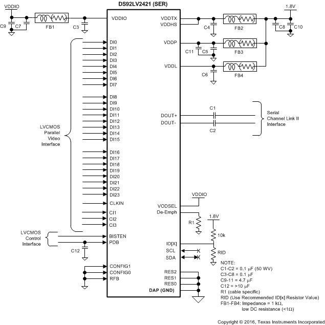 Figure 38. DS92LV2421 Typical Connection Diagram – Pin Control
8.2.1.1 Design Requirements
For this example, Table 18 lists the design parameters.
Table 18. Design Parameters
| PARAMETER | EXAMPLE VALUE | |||
|---|---|---|---|---|
| VDDIO | 1.8 V to 3.3 V | |||
| VDDL, VDDP, VDDHS, VDDTX | 1.8 V | |||
| AC-Coupling Capacitor for DOUT± | 100 nF | |||
8.2.1.2 Detailed Design Procedure
The DOUT± outputs require 100-nF AC-coupling capacitors to the line. The power supply filter capacitors are placed near the power supply pins. A smaller capacitance capacitor must be located closer to the power supply pins.
The VODSEL pin is tied to VDDIO for the long cable application. The de-emphasis pin may connect a resistor to ground. Refer to Table 3. The PDB and BISTEN pins are assumed to be controlled by a microprocessor. The PDB must remain in a low state until all power supply voltages reach the final voltage. The RFB pin is tied low to latch data on the falling edge of the PCLK and tied high for the rising clock edge. The CONFIG[1:0] pins are set depending on operating modes and backward compatibility. The SCL, SDA, and ID[X] pins are left open when these serial bus control pins are unused. The RES[2:0] pins and DAP must be tied to ground.
8.2.1.3 Application Curve
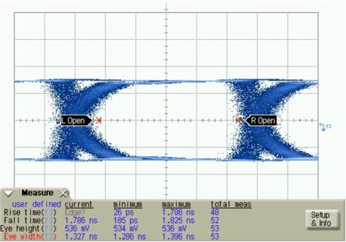 Figure 39. Eye Diagram at CLK = 20 MHz
8.2.2 DS92LV2422 Typical Connection
Figure 40 shows a typical application of the DS92LV2422 deserializer in pin or strap control mode for a 24-bit application. The LVDS inputs use 100-nF coupling capacitors to the line, and the receiver provides internal termination. Bypass capacitors are placed near the power supply pins. At a minimum, seven 0.1-µF capacitors and two 4.7-µF capacitors must be used for local device bypassing. System General Purpose Output (GPO) signals control the PDB and the BISTEN pins. In this application, the RFB pin is tied low to strobe the data on the falling edge of the CLKOUT.
Because the device is in pin or strap control mode, four 10-kΩ pullup resistors are used on the parallel output bus to select the desired device features. CONFIG[1:0] is set to 01'b for normal mode with control signal filter enabled, and this is accomplished with the strap pullup on DO23. The receiver input equalizer is also enabled and set to provide 7.5 dB of gain, and this is accomplished with EQ[3:0] set to 1001'b with strap pullups on DO12 and DO15. To reduce parallel bus EMI, the SSCG feature is enabled and set to fmod = CLK/2168 and ±1% with SSC[3:0] set to 0010'b and a strap pullup on DO4. The desired features are set with the use of the four pullup resistors.
The interface to the target display is with 3.3-V LVCMOS levels, thus the VDDIO pin is connected to the 3.3-V rail. The optional serial bus control is not used in this example, thus the SCL, SDA and ID[X] pins are left open. A delay cap is placed on the PDB signal to delay the enabling of the device until power is stable.
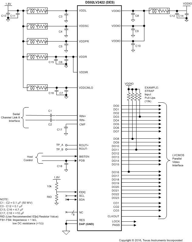 Figure 40. DS92LV2422 Typical Connection Diagram — Pin Control
8.2.2.1 Design Requirements
For this example, Table 19 lists the design parameters.
Table 19. Design Parameters
| PARAMETER | EXAMPLE VALUE | |||
|---|---|---|---|---|
| VDDIO | 1.8 V to 3.3 V | |||
| VDDL, VDDSC, VDDPR, VDDR, VDDIR, VDDCMLO |
1.8 V | |||
| AC-Coupling Capacitor for DOUT± | 100 nF | |||
8.2.2.2 Detailed Design Procedure
The RIN± inputs require 100-nF AC-coupling capacitors to the line. The power supply filter capacitors are placed near the power supply pins. A smaller capacitance capacitor must be placed closer to the power supply pins.
The device has 22 control and configuration pins that are called strap pins. These pins include an internal pulldown. For a high state, use a 10-kΩ resistor pullup to VDDIO.
The PDB and BISTEN pins are assumed to be controlled by a microprocessor. The PDB has to be in a low state until all power supply voltages reach the final voltage. The SCL, SDA, and ID[X] pins are left open when these serial bus control pins are unused.
The RES pin and DAP must be tied to ground.
8.2.2.3 Application Curves
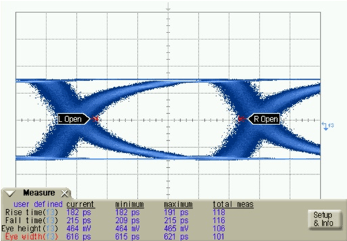 Figure 41. Eye Diagram at CLK = 45 MHz
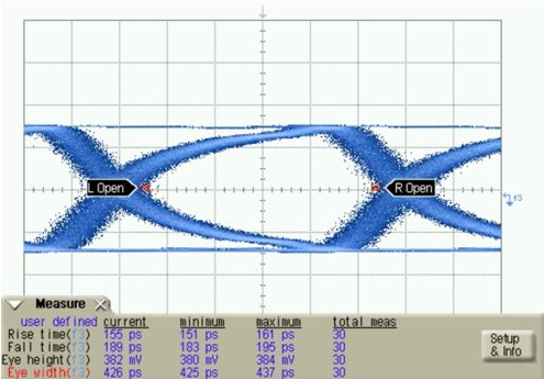 Figure 42. Eye Diagram at CLK = 65 MHz