SNOSB66B August 2011 – November 2014 EMB1412
PRODUCTION DATA.
- 1 Features
- 2 Applications
- 3 Description
- 4 Revision History
- 5 Pin Configuration and Functions
- 6 Specifications
- 7 Detailed Description
- 8 Layout
- 9 Device and Documentation Support
- 10Mechanical, Packaging, and Orderable Information
Package Options
Mechanical Data (Package|Pins)
- DGN|8
Thermal pad, mechanical data (Package|Pins)
- DGN|8
Orderable Information
6 Specifications
6.1 Absolute Maximum Ratings(1)
| MIN | MAX | UNIT | |
|---|---|---|---|
| VCC to VEE | −0.3 | 15 | V |
| VCC to IN_REF | −0.3 | 15 | V |
| IN/INB to IN_REF | −0.3 | 15 | V |
| IN_REF to VEE | −0.3 | 5 | V |
| Maximum junction temperature | 150 | °C |
(1) Stresses beyond those listed under Absolute Maximum Ratings may cause permanent damage to the device. These are stress ratings only, which do not imply functional operation of the device at these or any other conditions beyond those indicated under Recommended Operating Conditions. Exposure to absolute-maximum-rated conditions for extended periods may affect device reliability.
6.2 Handling Ratings
| MIN | MAX | UNIT | |||
|---|---|---|---|---|---|
| Tstg | Storage temperature range | –55 | 150 | °C | |
| V(ESD) | Electrostatic discharge | Human body model (HBM), per ANSI/ESDA/JEDEC JS-001, all pins(1) | 2 | kV | |
(1) JEDEC document JEP155 states that 500-V HBM allows safe manufacturing with a standard ESD control process.
6.3 Recommended Operating Conditions
over operating free-air temperature range (unless otherwise noted)| MIN | NOM | MAX | UNIT | ||
|---|---|---|---|---|---|
| Operating Junction Temperature | −40 | 125 | °C | ||
6.4 Thermal Information
| THERMAL METRIC(1) | EMB1412 | UNIT | |
|---|---|---|---|
| VSSOP (DGN) | |||
| 8 PINS | |||
| RθJA | Junction-to-ambient thermal resistance | 60(2) | °C/W |
| RθJCbot | Junction-to-case (bottom) thermal resistance | 4.7 | |
(1) For more information about traditional and new thermal metrics, see the IC Package Thermal Metrics application report, SPRA953.
(2) The primary goal of the thermal management is to maintain the integrated circuit (IC) junction temperature (TJ) below a specified limit to ensure reliable long term operation. The maximum TJ of IC components should be estimated in worst case operating conditions. The junction temperature can be calculated based on the power dissipated on the IC and the junction to ambient thermal resistance RθJA for the IC package in the application board and environment. The RθJA is not a given constant for the package and depends on the PCB design and the operating environment.
6.5 Electrical Characteristics
TJ = −40°C to 125°C, VCC = 12 V, INB = IN_REF = VEE = 0 V, No Load on output, unless otherwise specified.| PARAMETER | TEST CONDITIONS | MIN | TYP | MAX | UNIT | |
|---|---|---|---|---|---|---|
| SUPPLY | ||||||
| VCC | VCC Operating Range | VCC – IN_REF and VCC - VEE | 3.5 | 14 | V | |
| UVLO | VCC Under-voltage Lockout (rising) | VCC – IN_REF | 2.4 | 3.0 | 3.5 | V |
| VCCH | VCC Under-voltage Hysteresis | 230 | mV | |||
| ICC | VCC Supply Current | 1.0 | 2.0 | mA | ||
| CONTROL INPUTS | ||||||
| VIH | Logic High | 2.3 | V | |||
| VIL | Logic Low | 0.8 | V | |||
| VthH | High Threshold | 1.3 | 1.75 | 2.3 | V | |
| VthL | Low Threshold | 0.8 | 1.35 | 2.0 | V | |
| HYS | Input Hysteresis | 400 | mV | |||
| IIL | Input Current Low | IN = INB = 0 V | -1 | 0.1 | 1 | µA |
| IIH | Input Current High | IN = INB = VCC | -1 | 0.1 | 1 | µA |
| OUTPUT DRIVER | ||||||
| ROH | Output Resistance High | IOUT = -10 mA(1) | 30 | 50 | Ω | |
| ROL | Output Resistance Low | IOUT = 10 mA(1) | 1.4 | 2.5 | Ω | |
| ISOURCE | Peak Source Current | OUT = VCC/2, 200 ns pulsed current | 3 | A | ||
| ISINK | Peak Sink Current | OUT = VCC/2, 200 ns pulsed current | 7 | A | ||
| SWITCHING CHARACTERISTICS | ||||||
| td1 | Propagation Delay Time Low to High, IN/ INB rising ( IN to OUT) |
CLOAD = 2 nF | 25 | 40 | ns | |
| td2 | Propagation Delay Time High to Low, IN / INB falling (IN to OUT) |
CLOAD = 2 nF | 25 | 40 | ns | |
| tr | Rise time | CLOAD = 2 nF | 14 | ns | ||
| tf | Fall time | CLOAD = 2 nF | 12 | ns | ||
| LATCHUP PROTECTION | ||||||
| AEC –Q100, METHOD 004 | TJ = 150°C | 500 | mA | |||
| THERMAL RESISTANCE | ||||||
| RθJA | Junction to Ambient, 0 LFPM Air Flow |
VSSOP Package | 60 | °C/W | ||
| RθJC | Junction to Case | VSSOP Package | 4.7 | °C/W | ||
(1) The output resistance specification applies to the MOS device only. The total output current capability is the sum of the MOS and Bipolar devices.
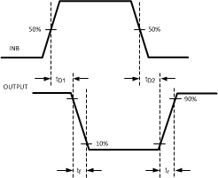 Figure 1. (A) Inverting
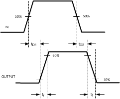 Figure 2. (B) Non-Inverting