SLAS907C December   2015  – December 2020 HD3SS214

PRODUCTION DATA  

  1. Features
  2. Applications
  3. Description
  4. Revision History
  5. Pin Configuration and Functions
  6. Specifications
    1. 6.1 Absolute Maximum Ratings (1) (1)
    2. 6.2 ESD Ratings
    3. 6.3 Recommended Operating Conditions
    4. 6.4 Thermal Information
    5. 6.5 Electrical Characteristics
    6. 6.6 Electrical Characteristics, Device Parameters
    7. 6.7 Timing Requirements
    8. 6.8 Typical Characteristics
  7. Detailed Description
    1. 7.1 Overview
    2. 7.2 Functional Block Diagram
    3. 7.3 Feature Description
      1. 7.3.1 High Speed Switching
      2. 7.3.2 HPD, AUX, and DDC Switching
      3. 7.3.3 Output Enable and Power Savings
    4. 7.4 Device Functional Modes
  8. Application and Implementation
    1. 8.1 Application Information
    2. 8.2 Typical Application
      1. 8.2.1 Dual GPU With Docking Station Support
      2. 8.2.2 Design Requirements
      3. 8.2.3 Detailed Design Procedure
        1. 8.2.3.1 DP Inputs
        2. 8.2.3.2 Source Selection Interface
      4. 8.2.4 DP++ Support
        1. 8.2.4.1 Design Requirements
        2. 8.2.4.2 Detailed Design Procedure
          1. 8.2.4.2.1 AUX and DDC Switching
          2. 8.2.4.2.2 CONFIG1 and CONFIG2 Routing
  9. Power Supply Recommendations
  10. 10Layout
    1. 10.1 Layout Guidelines
      1. 10.1.1 Layer Stack
      2. 10.1.2 Differential Traces
    2. 10.2 Layout Example
  11. 11Device and Documentation Support
    1. 11.1 Device Support
    2. 11.2 Receiving Notification of Documentation Updates
    3. 11.3 Community Resources
    4. 11.4 Trademarks
  12. 12Mechanical, Packaging, and Orderable Information

Package Options

Mechanical Data (Package|Pins)
Thermal pad, mechanical data (Package|Pins)
Orderable Information

Source Selection Interface

Two control pins on the HD3SS214 are responsible for selecting the incoming DP signal: Dx_SEL and AUX_SEL. Dx_SEL controls which high speed ports are selected. A low signal on Dx_SEL corresponds to Port A routed to Port C and a high signal corresponds to Port B routed to Port C. A slide switch is used to select the level for this signal. In an embedded application, this switch can be replaced by a GPIO signal from a microcontroller.

AUX channel is controlled by AUX_SEL. This pin configures the switch to route the incoming AUX signal to the outgoing AUX path, when AUX_SEL = 0 the AUXA channel will be routed to AUXC, when AUX_SEL = 1 the AUXB channel will be routed to AUXC. Figure 8-2 shows the selection circuitry.
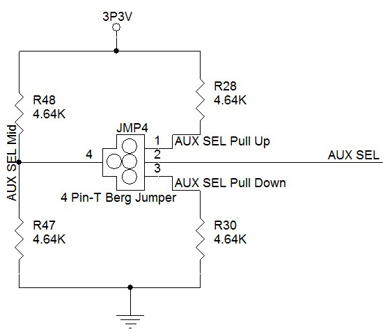
GUID-07B539E9-DE06-4280-AB09-572B7C09FB15-low.pngFigure 8-2 AUX_SEL Schematic