SLAS907C December 2015 – December 2020 HD3SS214
PRODUCTION DATA
- 1 Features
- 2 Applications
- 3 Description
- 4 Revision History
- 5 Pin Configuration and Functions
- 6 Specifications
- 7 Detailed Description
- 8 Application and Implementation
- 9 Power Supply Recommendations
- 10Layout
- 11Device and Documentation Support
- 12Mechanical, Packaging, and Orderable Information
Package Options
Mechanical Data (Package|Pins)
- ZXH|50
Thermal pad, mechanical data (Package|Pins)
Orderable Information
10.1.1 Layer Stack
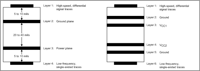
Routing the high-speed differential signal traces on the top layer avoids the use of vias (and the introduction of their inductances) and allows for clean interconnects from the DisplayPort connectors to the repeater inputs and from the repeater output to the subsequent receiver circuit.
Placing a solid ground plane next to the high-speed signal layer establishes controlled impedance for transmission line interconnects and provides an excellent low-inductance path for the return current flow.
Placing the power plane next to the ground plane creates additional high-frequency bypass capacitance.
Routing the fast-edged control signals on the bottom layer by prevents them from cross-talking into the high-speed signal traces and minimizes EMI.
If the receiver requires a supply voltage different from the one of the repeater, add a second power/ground plane system to the stack to keep it symmetrical. This makes the stack mechanically stable and prevents it from warping. Also, the power and ground plane of each power system can be placed closer together, thus increasing the high-frequency bypass capacitance significantly. Finally, a second power/ground system provides added isolation between the signal layers.
 Figure 10-1 Recommended 4- or 6- Layer (0.062") Stack for a Receiver PCB Design