SBOS378A March   2019  – November 2023 INA185

PRODUCTION DATA  

  1.   1
  2. Features
  3. Applications
  4. Description
  5. Pin Configuration and Functions
  6. Specifications
    1. 5.1 Absolute Maximum Ratings
    2. 5.2 ESD Ratings
    3. 5.3 Recommended Operating Conditions
    4. 5.4 Thermal Information
    5. 5.5 Electrical Characteristics
    6. 5.6 Typical Characteristics
  7. Detailed Description
    1. 6.1 Overview
    2. 6.2 Functional Block Diagrams
    3. 6.3 Feature Description
      1. 6.3.1 High Bandwidth and Slew Rate
      2. 6.3.2 Bidirectional Current Monitoring
      3. 6.3.3 Wide Input Common-Mode Voltage Range
      4. 6.3.4 Precise Low-Side Current Sensing
      5. 6.3.5 Rail-to-Rail Output Swing
    4. 6.4 Device Functional Modes
      1. 6.4.1 Normal Mode
      2. 6.4.2 Unidirectional Mode
      3. 6.4.3 Bidirectional Mode
      4. 6.4.4 Input Differential Overload
      5. 6.4.5 Shutdown Mode
  8. Application and Implementation
    1. 7.1 Application Information
      1. 7.1.1 Basic Connections
      2. 7.1.2 RSENSE and Device Gain Selection
      3. 7.1.3 Signal Filtering
    2. 7.2 Typical Application
      1. 7.2.1 Design Requirements
      2. 7.2.2 Detailed Design Procedure
      3. 7.2.3 Application Curve
    3. 7.3 Power Supply Recommendations
      1. 7.3.1 Common-Mode Transients Greater Than 26 V
    4. 7.4 Layout
      1. 7.4.1 Layout Guidelines
      2. 7.4.2 Layout Example
  9. Device and Documentation Support
    1. 8.1 Device Support
      1. 8.1.1 Development Support
    2. 8.2 Documentation Support
      1. 8.2.1 Related Documentation
    3. 8.3 Receiving Notification of Documentation Updates
    4. 8.4 Support Resources
    5. 8.5 Trademarks
    6. 8.6 Electrostatic Discharge Caution
    7. 8.7 Glossary
  10. Revision History
  11. 10Mechanical, Packaging, and Orderable Information

Package Options

Mechanical Data (Package|Pins)
Thermal pad, mechanical data (Package|Pins)
Orderable Information

Basic Connections

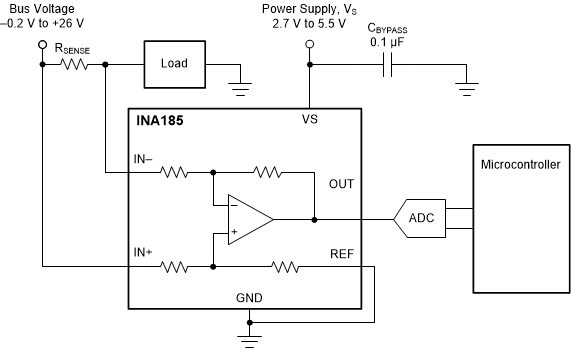
Figure 7-1 shows the basic connections of the INA185. Connect the input pins (IN+ and IN–) to the shunt resistor as close as possible to minimize any resistance in series with the shunt resistor.
GUID-9C2310ED-E91B-4618-9222-1467F4194CDB-low.gif
NOTE: To help eliminate ground offset errors between the device and the analog-to-digital converter (ADC), connect the REF pin to the ADC reference input and then to ground. For best performance, use an RC filter between the output of the INA185 and the ADC. See the Closed-Loop Analysis of Load-Induced Amplifier Stability Issues Using ZOUT application note for more details.
Figure 7-1 Basic Connections for the INA185

A power-supply bypass capacitor of at least 0.1 µF is required for proper operation. Applications with noisy or high-impedance power supplies can require additional decoupling capacitors to reject power-supply noise. Connect bypass capacitors close to the device pins.