SBOS386B May   2019  – March 2022 INA186-Q1

PRODUCTION DATA  

  1. Features
  2. Applications
  3. Description
  4. Revision History
  5. Pin Configuration and Functions
  6. Specifications
    1. 6.1 Absolute Maximum Ratings
    2. 6.2 ESD Ratings
    3. 6.3 Recommended Operating Conditions
    4. 6.4 Thermal Information
    5. 6.5 Electrical Characteristics
    6. 6.6 Typical Characteristics
  7. Detailed Description
    1. 7.1 Overview
    2. 7.2 Functional Block Diagram
    3. 7.3 Feature Description
      1. 7.3.1 Precision Current Measurement
      2. 7.3.2 Low Input Bias Current
      3. 7.3.3 Low Quiescent Current With Output Enable
      4. 7.3.4 Bidirectional Current Monitoring
      5. 7.3.5 High-Side and Low-Side Current Sensing
      6. 7.3.6 High Common-Mode Rejection
      7. 7.3.7 Rail-to-Rail Output Swing
    4. 7.4 Device Functional Modes
      1. 7.4.1 Normal Operation
      2. 7.4.2 Unidirectional Mode
      3. 7.4.3 Bidirectional Mode
      4. 7.4.4 Input Differential Overload
      5. 7.4.5 Shutdown
  8. Application and Implementation
    1. 8.1 Application Information
      1. 8.1.1 Basic Connections
      2. 8.1.2 RSENSE and Device Gain Selection
      3. 8.1.3 Signal Conditioning
      4. 8.1.4 Common-Mode Voltage Transients
    2. 8.2 Typical Applications
      1. 8.2.1 Design Requirements
      2. 8.2.2 Detailed Design Procedure
      3. 8.2.3 Application Curve
  9. Power Supply Recommendations
  10. 10Layout
    1. 10.1 Layout Guidelines
    2. 10.2 Layout Examples
  11. 11Device and Documentation Support
    1. 11.1 Documentation Support
      1. 11.1.1 Related Documentation
    2. 11.2 Receiving Notification of Documentation Updates
    3. 11.3 Support Resources
    4. 11.4 Trademarks
    5. 11.5 Electrostatic Discharge Caution
    6. 11.6 Glossary
  12. 12Mechanical, Packaging, and Orderable Information

Package Options

Mechanical Data (Package|Pins)
Thermal pad, mechanical data (Package|Pins)
Orderable Information

Detailed Design Procedure

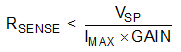
The maximum value of the current-sense resistor is calculated based on choice of gain, value of the maximum current the be sensed (IMAX), and the power-supply voltage (VS). When operating at the maximum current, the output voltage must not exceed the positive output swing specification, VSP. Using Equation 6, for the given design parameters the maximum value for RSENSE is calculated to be 1.321 kΩ.

Equation 6. GUID-0A3695C7-A6B2-4E97-8680-D4D11EE5FE94-low.gif

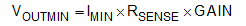
However, because this value exceeds the maximum recommended value for RSENSE, a resistance value of 1 kΩ must be used. When operating at the minimum current value, IMIN the output voltage must be greater than the swing to GND (VSN), specification. For this example, the output voltage at the minimum current is calculated using Equation 7 to be 25 mV, which is greater than the value for VSN.

Equation 7. GUID-6B5E2039-441D-4DCD-9ED6-EA2B07829960-low.gif