SBOS366E August 2006 – January 2021 INA193A-Q1 , INA194A-Q1 , INA195A-Q1 , INA196A-Q1 , INA197A-Q1 , INA198A-Q1
PRODUCTION DATA
- 1 Features
- 2 Applications
- 3 Description
- 4 Revision History
- 5 Pin Configuration and Functions
- 6 Specifications
- 7 Detailed Description
- 8 Application and Implementation
- 9 Power Supply Recommendations
- 10Layout
- 11Device and Documentation Support
- 12Mechanical, Packaging, and Orderable Information
Package Options
Mechanical Data (Package|Pins)
- DBV|5
Thermal pad, mechanical data (Package|Pins)
Orderable Information
7.4.1 Input Filtering
An obvious and straightforward location for filtering is at the output of the INA19xA series; however, this location negates the advantage of the low output impedance of the internal buffer. The only other option for filtering is at the input pins of the INA19xA, which is complicated by the internal 5-kΩ ± 30% input impedance (see Figure 7-6). Using the lowest possible resistor values minimizes both the initial shift in gain and effects of tolerance. The effect on initial gain is given by:
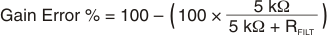
Total effect on gain error can be calculated by replacing the 5-kΩ term with 5 kΩ – 30% (or 3.5 kΩ) or 5 kΩ + 30% (or 6.5 kΩ). The tolerance extremes of RFILT can also be inserted into the equation. If a pair of 100-Ω 1% resistors are used on the inputs, the initial gain error is 1.96%. Worst-case tolerance conditions always occur at the lower excursion of the internal 5-kΩ resistor (3.5 kΩ), and the higher excursion of RFILT, 3% in this case.
The specified accuracy of the INA19xA must then be combined in addition to these tolerances. While this discussion treats accuracy worst-case conditions by combining the extremes of the resistor values, it is appropriate to use geometric mean or root sum square calculations to total the effects of accuracy variations.
") Figure 7-6 Input Filter (Gain Error = 1.5% to –2.2%)
Figure 7-6 Input Filter (Gain Error = 1.5% to –2.2%)