SBOS469H April   2009  – October 2023 INA199

PRODUCTION DATA  

  1.   1
  2. Features
  3. Applications
  4. Description
  5. Device Comparison Table
  6. Pin Configuration and Functions
  7. Specifications
    1. 6.1 Absolute Maximum Ratings
    2. 6.2 ESD Ratings
    3. 6.3 Recommended Operating Conditions
    4. 6.4 Thermal Information
    5. 6.5 Electrical Characteristics
    6. 6.6 Typical Characteristics
  8. Detailed Description
    1. 7.1 Overview
    2. 7.2 Functional Block Diagram
    3. 7.3 Feature Description
      1. 7.3.1 Basic Connections
      2. 7.3.2 Selecting RS
    4. 7.4 Device Functional Modes
      1. 7.4.1 Input Filtering
      2. 7.4.2 Shutting Down the INA199 Series
      3. 7.4.3 REF Input Impedance Effects
      4. 7.4.4 Using the INA199 With Common-Mode Transients Above 26 V
      5. 7.4.5 Improving Transient Robustness
  9. Application and Implementation
    1. 8.1 Application Information
    2. 8.2 Typical Applications
      1. 8.2.1 Unidirectional Operation
        1. 8.2.1.1 Design Requirements
        2. 8.2.1.2 Detailed Design Procedure
        3. 8.2.1.3 Application Curve
      2. 8.2.2 Bidirectional Operation
        1. 8.2.2.1 Design Requirements
        2. 8.2.2.2 Detailed Design Procedure
        3. 8.2.2.3 Application Curve
  10. Power Supply Recommendations
  11. 10Layout
    1. 10.1 Layout Guidelines
    2. 10.2 Layout Example
  12. 11Device and Documentation Support
    1. 11.1 Documentation Support
      1. 11.1.1 Related Documentation
    2. 11.2 Receiving Notification of Documentation Updates
    3. 11.3 Support Resources
    4. 11.4 Trademarks
    5. 11.5 Electrostatic Discharge Caution
    6. 11.6 Glossary
  13. 12Revision History
  14. 13Mechanical, Packaging, and Orderable Information

Package Options

Mechanical Data (Package|Pins)
Thermal pad, mechanical data (Package|Pins)
Orderable Information

Basic Connections

Figure 7-1 shows the basic connections for the INA199. The input pins, IN+ and IN–, must be connected as close as possible to the shunt resistor to minimize any resistance in series with the shunt resistor.
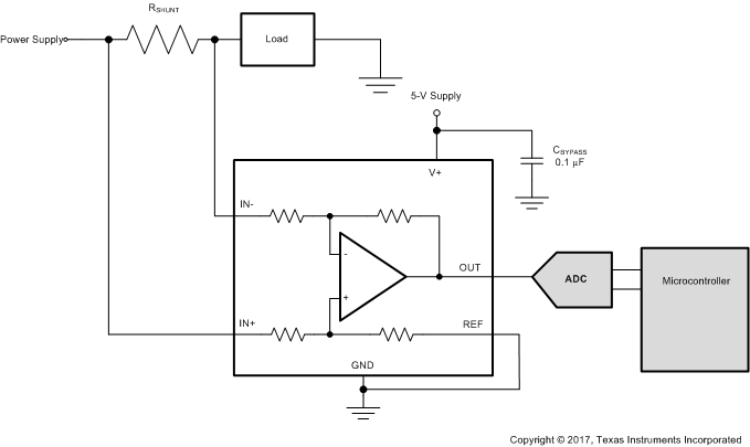
GUID-A9F6A9BF-8DB6-4321-AEF0-803F64119DBF-low.gifFigure 7-1 Typical Application

Power-supply bypass capacitors are required for stability. Applications with noisy or high-impedance power supplies may require additional decoupling capacitors to reject power-supply noise. Connect bypass capacitors close to the device pins.

On the RSW package, two pins are provided for each input. These pins must be tied together (that is, tie IN+ to IN+ and tie IN– to IN–).