SBOS469H April 2009 – October 2023 INA199
PRODUCTION DATA
- 1
- 1 Features
- 2 Applications
- 3 Description
- 4 Device Comparison Table
- 5 Pin Configuration and Functions
- 6 Specifications
- 7 Detailed Description
- 8 Application and Implementation
- 9 Power Supply Recommendations
- 10Layout
- 11Device and Documentation Support
- 12Revision History
- 13Mechanical, Packaging, and Orderable Information
Package Options
Mechanical Data (Package|Pins)
Thermal pad, mechanical data (Package|Pins)
- DCK|6
Orderable Information
7.4.3 REF Input Impedance Effects
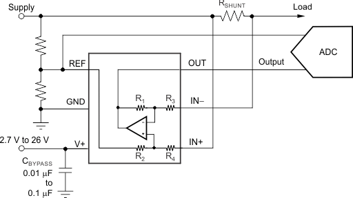
As with any difference amplifier, the INA199 series common-mode rejection ratio is affected by any impedance present at the REF input. This concern is not a problem when the REF pin is connected directly to most references or power supplies. When using resistive dividers from the power supply or a reference voltage, the REF pin must be buffered by an operational amplifier.
In systems where the INA199 output can be sensed differentially, such as by a differential input analog-to-digital converter (ADC) or by using two separate ADC inputs, the effects of external impedance on the REF input can be cancelled. Figure 7-4 depicts a method of taking the output from the INA199 by using the REF pin as a reference.
 Figure 7-4 Sensing the INA199 to Cancel Effects of Impedance on the REF Input