SBOS475K March 2009 – November 2023 INA210-Q1 , INA211-Q1 , INA212-Q1 , INA213-Q1 , INA214-Q1 , INA215-Q1
PRODUCTION DATA
- 1
- 1 Features
- 2 Applications
- 3 Description
- 4 Pin Configuration and Functions
- 5 Specifications
- 6 Detailed Description
- 7 Application and Implementation
- 8 Power Supply Recommendations
- 9 Layout
- 10Device and Documentation Support
- 11Revision History
- 12Mechanical, Packaging, and Orderable Information
Package Options
Mechanical Data (Package|Pins)
- DCK|6
Thermal pad, mechanical data (Package|Pins)
- DCK|6
Orderable Information
6.4.2 Shutting Down the INA21x-Q1 Series
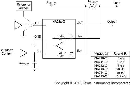
While the INA21x-Q1 family of devices does not have a shutdown pin, the low-power consumption of the device allows the output of a logic gate or transistor switch to power the device. This gate or switch turns on and turns off the INA21x-Q1 power-supply quiescent current.
However, in current-shunt monitoring applications, the amount of current drained from the shunt circuit in shutdown conditions must be considered. Evaluating this current drain involves considering the simplified schematic of the INA21x-Q1 family of devices in shutdown mode shown in Figure 6-3.

Slightly more than a 1-MΩ impedance (from the combination of 1-MΩ feedback and 5-kΩ input resistors) exists from each input of the INA21x-Q1 family of devices to the OUT pin and to the REF pin. The amount of current flowing through these pins depends on the respective ultimate connection. For example, if the REF pin is grounded, the calculation of the effect of the 1-MΩ impedance from the shunt to ground is straightforward. However, if the reference or operational amplifier (op amp) is powered when the INA21x-Q1 family of devices is shut down, the calculation is direct. Instead of assuming 1 MΩ to ground, however, assume 1 MΩ to the reference voltage. If the reference or op amp is also shut down, some knowledge of the reference or op amp output impedance under shutdown conditions is required. For instance, if the reference source behaves as an open circuit when not powered, little or no current flows through the 1-MΩ path.
Regarding the 1-MΩ path to the output pin, the output stage of a disabled INA21x-Q1 device does constitute a good path to ground; consequently, this current is directly proportional to a shunt common-mode voltage present across a 1-MΩ resistor.
When the device is powered up, an additional, nearly constant and well-matched 25-µA current flows in each of the inputs as long as the shunt common-mode voltage is 3 V or higher. Below 2-V common-mode, the only current effects are the result of the 1-MΩ resistors.