SBOS475K March 2009 – November 2023 INA210-Q1 , INA211-Q1 , INA212-Q1 , INA213-Q1 , INA214-Q1 , INA215-Q1
PRODUCTION DATA
- 1
- 1 Features
- 2 Applications
- 3 Description
- 4 Pin Configuration and Functions
- 5 Specifications
- 6 Detailed Description
- 7 Application and Implementation
- 8 Power Supply Recommendations
- 9 Layout
- 10Device and Documentation Support
- 11Revision History
- 12Mechanical, Packaging, and Orderable Information
Package Options
Mechanical Data (Package|Pins)
- DCK|6
Thermal pad, mechanical data (Package|Pins)
Orderable Information
6.4.5 Improving Transient Robustness
Applications involving large input transients with excessive dV/dt above 2 kV per microsecond present at the device input pins can cause damage to the internal ESD structures on version A devices.
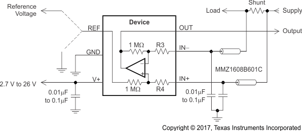
The potential damage from large input transients is a result of the internal latching of the ESD structure to ground when this transient occurs at the input. With significant current available in most current-sensing applications, the large current flowing through the input transient-triggered, ground-shorted ESD structure quickly results in damage to the silicon. External filtering can be used to attenuate the transient signal prior to reaching the inputs to avoid the latching condition. Care must be taken to ensure that external series input resistance does not significantly impact gain error accuracy. For accuracy purposes, keep these resistances under 10 Ω if possible. Ferrite beads are recommended for this filter because of the inherently low-dc ohmic value. Ferrite beads with less than 10 Ω of resistance at dc and over 600 Ω of resistance at 100 MHz to 200 MHz are recommended. The recommended capacitor values for this filter are between 0.01 µF and 0.1 µF to ensure adequate attenuation in the high-frequency region. Figure 6-7 illustrates this protection scheme.
 Figure 6-7 Transient Protection
To minimize the cost of adding these external components to protect the device in applications where large transient signals may be present, version B and C devices are now available with new ESD structures that are not susceptible to this latching condition. Version B and C devices are incapable of sustaining these damage-causing latched conditions so they do not have the same sensitivity to the transients that the version A devices have, thus making the version B and C devices a better fit for these applications.