SBOS448G August 2008 – December 2015 INA219
PRODUCTION DATA.
- 1 Features
- 2 Applications
- 3 Description
- 4 Revision History
- 5 Related Products
- 6 Pin Configuration and Functions
- 7 Specifications
-
8 Detailed Description
- 8.1 Overview
- 8.2 Functional Block Diagram
- 8.3 Feature Description
- 8.4 Device Functional Modes
- 8.5 Programming
- 8.6 Register Maps
- 9 Application and Implementation
- 10Power Supply Recommendations
- 11Layout
- 12Device and Documentation Support
- 13Mechanical, Packaging, and Orderable Information
Package Options
Mechanical Data (Package|Pins)
Thermal pad, mechanical data (Package|Pins)
- DCN|8
Orderable Information
9 Application and Implementation
NOTE
Information in the following applications sections is not part of the TI component specification, and TI does not warrant its accuracy or completeness. TI’s customers are responsible for determining suitability of components for their purposes. Customers should validate and test their design implementation to confirm system functionality.
9.1 Application Information
The INA219 is a current shunt and power monitor with an I2C- and SMBus-compatible interface. The device monitors both a shunt voltage drop and bus supply voltage. Programmable calibration value, combined with an internal multiplier, enable readouts of current and power.
9.2 Typical Application
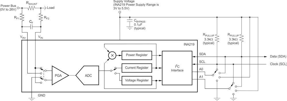
Figure 28 shows a typical application circuit for the INA219. Use a 0.1-μF ceramic capacitor for power-supply bypassing, placed as closely as possible to the supply and ground pins.
The input filter circuit consisting of RF1, RF2, and CF is not necessary in most applications. If the need for filtering is unknown, reserve board space for the components and install 0-Ω resistors for RF1 and RF2 and leave CF unpopulated, unless a filter is needed (see Filtering and Input Considerations).
The pull-up resistors shown on the SDA and SCL lines are not needed if there are pullup resistors on these same lines elsewhere in the system. Resistor values shown are typical: consult either the I2C or SMBus specification to determine the acceptable minimum or maximum values and also refer to the Specifications for Output Current Limitations.
 Figure 28. Typical Application Circuit
9.2.1 Design Requirements
The INA219 measures the voltage across a current-sensing resistor (RSHUNT) when current passes through the resistor. The device also measures the bus supply voltage, and calculates power when calibrated. This section goes through the steps to program the device for power measurements, and shows the register results Table 8.
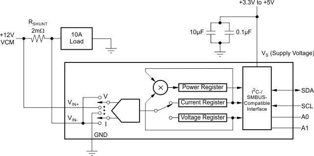
The Conditions for the example circuit is: Maximum expected load current = 15 A, Nominal load current = 10 A, VCM = 12 V, RSHUNT = 2 mΩ, VSHUNT FSR = 40 mV (PGA = /1), and BRNG = 0 (VBUS range = 16 V).
9.2.2 Detailed Design Procedure
Figure 29 shows a nominal 10-A load that creates a differential voltage of 20 mV across a 2-mΩ shunt resistor. The common mode is at 12 volts and the voltage present at the IN– pin is equal to the common-mode voltage minus the differential drop across the resistor.
For this example, the minimum-current LSB is calculated to be 457.78 µA/bit, assuming a maximum expected current of 15 A using Equation 2. This value is rounded up to 1 mA/bit and is chosen for the current LSB. Setting the current LSB to this value allows for sufficient precision while serving to simplify the math as well. Using Equation 1 results in a calibration value of 20480 (5000h). This value is then programmed into the Calibration register.
 Figure 29. Example Circuit Configuration
The bus voltage is internally measured at the IN– pin to calculate the voltage level delivered to the load. The Bus Voltage register bits are not right-aligned; therefore, they must be shifted right by three bits. Multiply the shifted contents by the 4-mV LSB to compute the bus voltage measured by the device in volts. The shifted value of the Bus Voltage register contents is equal to BB3h, the decimal equivalent of 2995. This value of 2995 is multiplied by the 4-mV LSB, and results in a value of 11.98 V. As shown, the voltage at the IN– pin is 11.98 V. For a 40-mV, full-scale range, this small difference is not a significant deviation from the 12-V common-mode voltage. However, at larger full-scale ranges, this deviation can be much larger.
The Current register content is internally calculated using Equation 4, and the result of 10000 (2710h) is automatically loaded into the register. Current in amperes is equal to 1 mA/bit times 10000, and results in a 10-A load current.
The Power register content is internally calculated using Equation 5 and the result of 5990 (1766h) is automatically loaded into the register. Multiplying this result by the Power register LSB 20 × 10–3(20 times 1 × 10–3 current LSB using Equation 3), results in a power calculation of 5990 × 20 mW/bit, and equals 119.8 W. This result matches what is expected for this register. A calculation for the power delivered to the load uses 11.98 V (12 VCM – 20-mV shunt drop) multiplied by the load current of 10 A to give a 119.8-W result.
9.2.2.1 Register Results for the Example Circuit
Table 8 shows the register readings for the Calibration example.
Table 8. Register Results(1)
| REGISTER NAME | ADDRESS | CONTENTS | ADJ | DEC | LSB | VALUE |
|---|---|---|---|---|---|---|
| Configuration | 00h | 019Fh | ||||
| Shunt | 01h | 07D0h | 2000 | 10 µV | 20 mV | |
| Bus | 02h | 5D98h | 0BB3 | 2995 | 4 mV | 11.98 V |
| Calibration | 05h | 5000h | 20480 | |||
| Current | 04h | 2710h | 10000 | 1 mA | 10.0 A | |
| Power | 03h | 1766h | 5990 | 20 mW | 119.8 W |