SBOS448G August   2008  – December 2015 INA219

PRODUCTION DATA.  

  1. Features
  2. Applications
  3. Description
  4. Revision History
  5. Related Products
  6. Pin Configuration and Functions
  7. Specifications
    1. 7.1 Absolute Maximum Ratings
    2. 7.2 ESD Ratings
    3. 7.3 Recommended Operating Conditions
    4. 7.4 Thermal Information
    5. 7.5 Electrical Characteristics:
    6. 7.6 Bus Timing Diagram Definitions
    7. 7.7 Typical Characteristics
  8. Detailed Description
    1. 8.1 Overview
    2. 8.2 Functional Block Diagram
    3. 8.3 Feature Description
      1. 8.3.1 Basic ADC Functions
        1. 8.3.1.1 Power Measurement
        2. 8.3.1.2 PGA Function
        3. 8.3.1.3 Compatibility With TI Hot Swap Controllers
    4. 8.4 Device Functional Modes
      1. 8.4.1 Filtering and Input Considerations
    5. 8.5 Programming
      1. 8.5.1 Programming the Calibration Register
      2. 8.5.2 Programming the Power Measurement Engine
        1. 8.5.2.1 Calibration Register and Scaling
      3. 8.5.3 Simple Current Shunt Monitor Usage (No Programming Necessary)
      4. 8.5.4 Default Settings
      5. 8.5.5 Bus Overview
        1. 8.5.5.1 Serial Bus Address
        2. 8.5.5.2 Serial Interface
      6. 8.5.6 Writing to and Reading from the INA219
        1. 8.5.6.1 High-Speed I2C Mode
        2. 8.5.6.2 Power-Up Conditions
    6. 8.6 Register Maps
      1. 8.6.1 Register Information
      2. 8.6.2 Register Details
        1. 8.6.2.1 Configuration Register (address = 00h) [reset = 399Fh]
      3. 8.6.3 Data Output Registers
        1. 8.6.3.1 Shunt Voltage Register (address = 01h)
        2. 8.6.3.2 Bus Voltage Register (address = 02h)
        3. 8.6.3.3 Power Register (address = 03h) [reset = 00h]
        4. 8.6.3.4 Current Register (address = 04h) [reset = 00h]
      4. 8.6.4 Calibration Register
        1. 8.6.4.1 Calibration Register (address = 05h) [reset = 00h]
  9. Application and Implementation
    1. 9.1 Application Information
    2. 9.2 Typical Application
      1. 9.2.1 Design Requirements
      2. 9.2.2 Detailed Design Procedure
        1. 9.2.2.1 Register Results for the Example Circuit
  10. 10Power Supply Recommendations
  11. 11Layout
    1. 11.1 Layout Guidelines
    2. 11.2 Layout Example
  12. 12Device and Documentation Support
    1. 12.1 Community Resources
    2. 12.2 Trademarks
    3. 12.3 Electrostatic Discharge Caution
    4. 12.4 Glossary
  13. 13Mechanical, Packaging, and Orderable Information

Package Options

Mechanical Data (Package|Pins)
Thermal pad, mechanical data (Package|Pins)
Orderable Information

11 Layout

11.1 Layout Guidelines

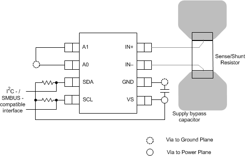
Connect the input pins (IN+ and IN–) to the sensing resistor using a Kelvin connection or a 4-wire connection. These connection techniques ensure that only the current-sensing resistor impedance is detected between the input pins. Poor routing of the current-sensing resistor commonly results in additional resistance present between the input pins. Given the very low ohmic value of the current-sensing resistor, any additional high-current carrying impedance causes significant measurement errors. Place the power-supply bypass capacitor as close as possible to the supply and ground pins.

11.2 Layout Example
INA219 ai_recommended-layout_sbos448.gif Figure 30. Recommended Layout