SBOS644D February 2013 – July 2022 INA231
PRODUCTION DATA
- 1 Features
- 2 Applications
- 3 Description
- 4 Revision History
- 5 Device Comparison
- 6 Pin Configuration and Functions
- 7 Specifications
-
8 Detailed Description
- 8.1 Overview
- 8.2 Functional Block Diagram
- 8.3 Feature Description
- 8.4 Device Functional Modes
- 8.5 Programming
- 8.6
Register Maps
- 8.6.1 Configuration Register (00h, Read/Write)
- 8.6.2 Shunt Voltage Register (01h, Read-Only)
- 8.6.3 Bus Voltage Register (02h, Read-Only)
- 8.6.4 Power Register (03h, Read-Only)
- 8.6.5 Current Register (04h, Read-Only)
- 8.6.6 Calibration Register (05h, Read/Write)
- 8.6.7 Mask/Enable Register (06h, Read/Write)
- 8.6.8 Alert Limit Register (07h, Read/Write)
- 9 Application and Implementation
- 10Device and Documentation Support
- 11Mechanical, Packaging, and Orderable Information
Package Options
Refer to the PDF data sheet for device specific package drawings
Mechanical Data (Package|Pins)
- YFF|12
- YFD|12
Thermal pad, mechanical data (Package|Pins)
Orderable Information
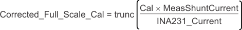
8.5.2.1 Calibration Register and Scaling
The Calibration register makes it possible to set the scaling of the Current and Power registers to the values that are most useful for a given application. One strategy may be to set the Calibration register so that the largest possible number is generated in the Current register or Power register at the expected full-scale point. This approach yields the highest resolution based on the previously-calculated minimum Current_LSB in the equation for the Calibration register (Equation 1). The Calibration register can also be selected to provide values in the Current and Power registers that either provide direct decimal equivalents of the values being measured, or yield a round LSB value for each corresponding register. After these choices have been made, the Calibration register also offers possibilities for end-user, system-level calibration. By physically measuring the current with an external ammeter, the exact current is known. The value of the Calibration register can then be adjusted based on the measured current result of the INA231 to cancel the total system error, as shown in Equation 5.