SBOS662C July   2016  – December 2021 INA240

PRODUCTION DATA  

  1. Features
  2. Applications
  3. Description
  4. Revision History
  5. Device Comparison
  6. Pin Configuration and Functions
  7. Specifications
    1. 7.1 Absolute Maximum Ratings
    2. 7.2 ESD Ratings
    3. 7.3 Recommended Operating Conditions
    4. 7.4 Thermal Information
    5. 7.5 Electrical Characteristics
    6. 7.6 Typical Characteristics
  8. Detailed Description
    1. 8.1 Overview
    2. 8.2 Functional Block Diagram
    3. 8.3 Feature Description
      1. 8.3.1 Amplifier Input Signal
        1. 8.3.1.1 Enhanced PWM Rejection Operation
        2. 8.3.1.2 Input Signal Bandwidth
      2. 8.3.2 Selecting the Sense Resistor (RSENSE)
    4. 8.4 Device Functional Modes
      1. 8.4.1 Adjusting the Output Midpoint With the Reference Pins
      2. 8.4.2 Reference Pin Connections for Unidirectional Current Measurements
        1. 8.4.2.1 Ground Referenced Output
        2. 8.4.2.2 VS Referenced Output
      3. 8.4.3 Reference Pin Connections for Bidirectional Current Measurements
        1. 8.4.3.1 Output Set to External Reference Voltage
        2. 8.4.3.2 Output Set to Midsupply Voltage
        3. 8.4.3.3 Output Set to Mid-External Reference
        4. 8.4.3.4 Output Set Using Resistor Divider
      4. 8.4.4 Calculating Total Error
        1. 8.4.4.1 Error Sources
        2. 8.4.4.2 Reference Voltage Rejection Ratio Error
          1. 8.4.4.2.1 Total Error Example 1
          2. 8.4.4.2.2 Total Error Example 2
  9. Application and Implementation
    1. 9.1 Application Information
      1. 9.1.1 Input Filtering
    2. 9.2 Typical Applications
      1. 9.2.1 Inline Motor Current-Sense Application
        1. 9.2.1.1 Design Requirements
        2. 9.2.1.2 Detailed Design Procedure
        3. 9.2.1.3 Application Curve
      2. 9.2.2 Solenoid Drive Current-Sense Application
        1. 9.2.2.1 Design Requirements
        2. 9.2.2.2 Detailed Design Procedure
        3. 9.2.2.3 Application Curve
    3. 9.3 What to Do and What Not to Do
      1. 9.3.1 High-Precision Applications
      2. 9.3.2 Kelvin Connection from the Current-Sense Resistor
  10. 10Power Supply Recommendations
    1. 10.1 Power Supply Decoupling
  11. 11Layout
    1. 11.1 Layout Guidelines
      1. 11.1.1 Connection to the Current-Sense Resistor
    2. 11.2 Layout Example
  12. 12Device and Documentation Support
    1. 12.1 Documentation Support
      1. 12.1.1 Related Documentation
    2. 12.2 Receiving Notification of Documentation Updates
    3. 12.3 Support Resources
    4. 12.4 Trademarks
    5. 12.5 Electrostatic Discharge Caution
    6. 12.6 Glossary
  13. 13Mechanical, Packaging, and Orderable Information

Package Options

Mechanical Data (Package|Pins)
Thermal pad, mechanical data (Package|Pins)
Orderable Information

Description

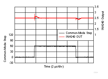
The INA240 device is a voltage-output, current-sense amplifier with enhanced PWM rejection that can sense drops across shunt resistors over a wide common-mode voltage range from –4 V to 80 V, independent of the supply voltage. The negative common-mode voltage allows the device to operate below ground, accommodating the flyback period of typical solenoid applications. Enhanced PWM rejection provides high levels of suppression for large common-mode transients (ΔV/Δt) in systems that use pulse width modulation (PWM) signals (such as motor drives and solenoid control systems). This feature allows for accurate current measurements without large transients and associated recovery ripple on the output voltage.

This device operates from a single 2.7-V to 5.5-V power supply, drawing a maximum of 2.4 mA of supply current. Four fixed gains are available: 20 V/V, 50 V/V, 100 V/V, and 200 V/V. The low offset of the zero-drift architecture enables current sensing with maximum drops across the shunt as low as 10-mV full-scale. All versions are specified over the extended operating temperature range (–40°C to +125°C), and are offered in an 8-pin TSSOP and 8-pin SOIC packages.

Device Information(1)
PART NUMBERPACKAGEBODY SIZE (NOM)
INA240TSSOP (8)3.00 mm × 4.40 mm
SOIC (8)4.90 mm × 3.91 mm
For all available packages, see the package option addendum at the end of the data sheet.
GUID-2E2A4C3D-A872-4E82-9784-372B1A0145E2-low.gif Enhanced PWM Rejection