SBOSAA0C november 2021 – may 2023 INA350
PRODUCTION DATA
- 1
- 1 Features
- 2 Applications
- 3 Description
- 4 Revision History
- 5 Device Comparison Table
- 6 Pin Configuration and Functions
- 7 Specifications
- 8 Detailed Description
- 9 Application and Implementation
- 10Device and Documentation Support
- 11Mechanical, Packaging, and Orderable Information
Package Options
Mechanical Data (Package|Pins)
Thermal pad, mechanical data (Package|Pins)
- DSG|8
Orderable Information
9.2.1.2 Detailed Design Procedure
This section provides basic calculations to lay out the instrumentation amplifier with respect to the given design requirements.
One of the key considerations in resistive-bridge sensors is the common-mode voltage, VCM. If the bridge is balanced (no pressure, thus no voltage change), VCM(zero) is half of the bridge excitation (VEXT). In this example VCM (zero) is 2.5 V. For the maximum pressure of 12 psi, the bridge common-mode voltage, VCM(MAX), is calculated by:
where
Thus, the maximum common-mode voltage applied results in:
Similarly, the minimum common-mode voltage can be calculated as,
The next step is to calculate the gain required for the given maximum sensor output voltage span, VDIFF, in respect to the required VOUT, which is the full-scale range of the ADC.
The following equation calculates the gain value using the maximum input voltage and the required output voltage:
Considering, INA350 is a selectable gain INA with gain options of 10, 20, 30, 50, the INA350ABS with GS tied high enables G = 20 ensuring the maximum output signal swing for the ADC.
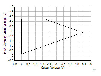
Next, let us make sure that the INA350 can operate within this range checking the Input Common-Mode Voltage vs Output Voltage curves in the Typical Characteristics section. The relevant figure is also in this section for convenience. Looking at Figure 9-63, we can confirm that a output signal swing of 3 V is supported for the input signal swing between 2.425 V and 2.575 V, thus making sure of the linear operation.

| VS = 5.5 V | G = 10, 20, 30, 50 | VREF = 0 V |
Additional series resistor in the Wheatstone bridge string (R1) may or may not be required. This is decided based on the intended output voltage swing for a particular combination of supply voltage, reference voltage and the selected gain for an input common mode voltage range. R1 helps adjust the input common-mode voltage range, and thus can help accommodate the intended output voltage swing. In this particular example, it are not required and can be shorted out.