SBOS894A April   2019  – June 2019 INA818

PRODUCTION DATA.  

  1. Features
  2. Applications
  3. Description
    1.     Device Images
      1.      INA818 Simplified Internal Schematic
      2.      Typical Distribution of Input Stage Offset Voltage Drift
  4. Revision History
  5. Device Comparison Table
  6. Pin Configuration and Functions
    1.     Pin Functions
  7. Specifications
    1. 7.1 Absolute Maximum Ratings
    2. 7.2 ESD Ratings
    3. 7.3 Recommended Operating Conditions
    4. 7.4 Thermal Information
    5. 7.5 Electrical Characteristics
    6. 7.6 Typical Characteristics: Table of Graphs
    7. 7.7 Typical Characteristics
  8. Detailed Description
    1. 8.1 Overview
    2. 8.2 Functional Block Diagram
    3. 8.3 Feature Description
      1. 8.3.1 Setting the Gain
        1. 8.3.1.1 Gain Drift
      2. 8.3.2 EMI Rejection
      3. 8.3.3 Input Common-Mode Range
      4. 8.3.4 Input Protection
      5. 8.3.5 Operating Voltage
      6. 8.3.6 Error Sources
    4. 8.4 Device Functional Modes
  9. Application and Implementation
    1. 9.1 Application Information
      1. 9.1.1 Reference Pin
      2. 9.1.2 Input Bias Current Return Path
    2. 9.2 Typical Applications
      1. 9.2.1 Three-Pin Programmable Logic Controller (PLC)
        1. 9.2.1.1 Design Requirements
        2. 9.2.1.2 Detailed Design Procedure
        3. 9.2.1.3 Application Curves
      2. 9.2.2 Resistance Temperature Detector Interface
  10. 10Power Supply Recommendations
  11. 11Layout
    1. 11.1 Layout Guidelines
    2. 11.2 Layout Example
  12. 12Device and Documentation Support
    1. 12.1 Documentation Support
      1. 12.1.1 Related Documentation
    2. 12.2 Receiving Notification of Documentation Updates
    3. 12.3 Community Resources
    4. 12.4 Trademarks
    5. 12.5 Electrostatic Discharge Caution
    6. 12.6 Glossary
  13. 13Mechanical, Packaging, and Orderable Information

Package Options

Mechanical Data (Package|Pins)
Thermal pad, mechanical data (Package|Pins)
Orderable Information

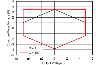
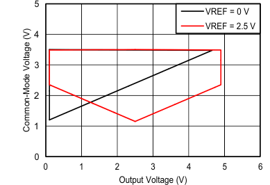
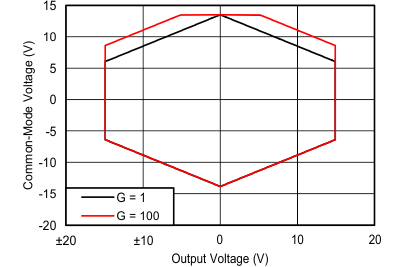
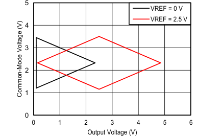
Input Common-Mode Range

The linear input voltage range of the INA818 input circuitry extends within 1.5 V (typical) of both power supplies and maintains excellent common-mode rejection throughout this range. The common-mode range for the most common operating conditions are shown in Figure 58, Figure 53, and Figure 54. The common-mode range for other operating conditions is best calculated using the Common-Mode Input Range Calculator for Instrumentation Amplifiers.
INA818 D054_SBOS959.gif
VS = 5 V G = 1
Figure 58. Input Common-Mode Voltage vs Output Voltage
INA818 D055_SBOS959.gif
VS = ±5 V VREF = 0 V
Figure 60. Input Common-Mode Voltage vs Output Voltage
INA818 D056_SBOS959.gif
VS = 5 V G = 100
Figure 59. Input Common-Mode Voltage vs Output Voltage
INA818 D052_SBOS959.gif
VS = ±15 V VREF = 0 V
Figure 61. Input Common-Mode Voltage vs Output Voltage