SBOS894A April 2019 – June 2019 INA818
PRODUCTION DATA.
- 1 Features
- 2 Applications
- 3 Description
- 4 Revision History
- 5 Device Comparison Table
- 6 Pin Configuration and Functions
- 7 Specifications
- 8 Detailed Description
- 9 Application and Implementation
- 10Power Supply Recommendations
- 11Layout
- 12Device and Documentation Support
- 13Mechanical, Packaging, and Orderable Information
Package Options
Mechanical Data (Package|Pins)
- D|8
Thermal pad, mechanical data (Package|Pins)
Orderable Information
9.1.1 Reference Pin
The output voltage of the INA818 is developed with respect to the voltage on the reference pin, REF. In dual-supply operation, REF (pin 6) is connected to the low-impedance system ground. In single-supply operation, offsetting the output signal to a precise midsupply level is useful (for example, 2.5 V in a 5-V supply environment). To accomplish this level shift, a voltage source must be connected to the REF pin to level-shift the output so that the INA818 drives a single-supply ADC.
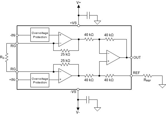
The voltage source applied to the reference pin must have a low output impedance. As shown in Figure 65, any resistance at the reference pin (shown as RREF in Figure 65) is in series with an internal 40-kΩ resistor.
 Figure 65. Parasitic Resistance Shown at the Reference Pin
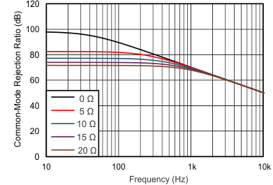
 The parasitic resistance at the reference pin (RREF) creates an imbalance in the four resistors of the internal difference amplifier, which degrades the common-mode rejection ratio (CMRR). Figure 66 shows the degradation in CMRR of the INA818 as a result of increased resistance at the reference pin. For the best performance, keep the source impedance to the REF pin (RREF) below 5 Ω.
 Figure 66. The Effect of Increasing Resistance at the Reference Pin
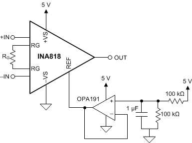
 Voltage-reference devices are a suitable option for providing a low-impedance voltage source for the reference pin. However, if a resistor voltage divider generates a reference voltage, the divider must be buffered by an op amp, as Figure 67 shows, in order to avoid CMRR degradation.
 Figure 67. Using an Op Amp to Buffer Reference Voltages