SBOSA75B July 2021 – November 2021 INA823
PRODUCTION DATA
- 1 Features
- 2 Applications
- 3 Description
- 4 Revision History
- 5 Device Comparison Table
- 6 Pin Configuration and Functions
- 7 Specifications
- 8 Detailed Description
- 9 Application and Implementation
- 10Power Supply Recommendations
- 11Layout
- 12Device and Documentation Support
- 13Mechanical, Packaging, and Orderable Information
Package Options
Mechanical Data (Package|Pins)
Thermal pad, mechanical data (Package|Pins)
Orderable Information
7.6 Typical Characteristics
at TA = 25°C, VS = ±15 V, RL = 10 kΩ, CL = 0 pF, VCM = VREF = 0 V, and G = 1 (unless otherwise noted)
Table 7-1 Table of Graphs
| FIGURE TITLE | FIGURE NUMBER |
|---|---|
| Typical Distribution Graphs | |
| Typical Distribution of Input Stage Offset Voltage | Figure 7-1 |
| Typical Distribution of Input Stage Offset Voltage Drift | Figure 7-2 |
| Typical Distribution of Output Stage Offset Voltage | Figure 7-3 |
| Typical Distribution of Output Stage Offset Voltage Drift | Figure 7-4 |
| Typical Distribution of Inverting Input Bias Current | Figure 7-5 |
| Typical Distribution of Noninverting Input Bias Current | Figure 7-6 |
| Typical Distribution of Input Offset Current | Figure 7-7 |
| Typical CMRR Distribution, G = 1 | Figure 7-8 |
| Typical CMRR Distribution, G = 10 | Figure 7-9 |
| Typical Gain Error Distribution | Figure 7-10 |
| vs Temperature Graphs | |
| Input Stage Offset Voltage vs Temperature | Figure 7-11 |
| Output Stage Offset Voltage vs Temperature | Figure 7-12 |
| Input Bias Current vs Temperature | Figure 7-13 |
| Input Offset Current vs Temperature | Figure 7-14 |
| CMRR vs Temperature, G = 1 | Figure 7-15 |
| CMRR vs Temperature, G = 10 | Figure 7-16 |
| Gain Error vs Temperature, G = 1 | Figure 7-17 |
| Gain Error vs Temperature, G = 100 | Figure 7-18 |
| Supply Current vs Temperature | Figure 7-19 |
| AC Performance Graphs | |
| Closed-Loop Gain vs Frequency | Figure 7-20 |
| CMRR vs Frequency (RTI) | Figure 7-21 |
| CMRR vs Frequency (RTI, 1-kΩ source imbalance) | Figure 7-22 |
| Positive PSRR vs Frequency (RTI) | Figure 7-23 |
| Negative PSRR vs Frequency (RTI) | Figure 7-24 |
| Voltage Noise Spectral Density vs Frequency (RTI) | Figure 7-25 |
| Current Noise Spectral Density vs Frequency (RTI) | Figure 7-26 |
| 0.1-Hz to 10-Hz RTI Voltage Noise | Figure 7-27 |
| 0.1-Hz to 10-Hz RTI Voltage Noise, G = 1000 | Figure 7-28 |
| Small-Signal Response, G = 1 | Figure 7-29 |
| Small-Signal Response, G = 10 | Figure 7-30 |
| Small-Signal Response, G = 100 | Figure 7-31 |
| Small-Signal Response, G = 1000 | Figure 7-32 |
| Overshoot vs Capacitive Loads | Figure 7-33 |
| Large-Signal Step Response | Figure 7-34 |
| Settling Time vs Step Size | Figure 7-35 |
| Large-Signal Frequency Response | Figure 7-36 |
| Closed-Loop Output Impedance vs Frequency | Figure 7-37 |
| Input and Output Voltage Graphs | |
| Input Current vs Input Overvoltage | Figure 7-38 |
| Gain Nonlinearity, G = 1 | Figure 7-39 |
| Gain Nonlinearity, G = 10 | Figure 7-40 |
| Gain Nonlinearity, G = 100 | Figure 7-41 |
| Gain Nonlinearity, G = 1000 | Figure 7-42 |
| Positive Input Bias Current vs Common‑Mode Voltage (VS–) | Figure 7-43 |
| Positive Input Bias Current vs Common‑Mode Voltage (VS+) | Figure 7-44 |
| Negative Input Bias Current vs Common‑Mode Voltage (VS–) | Figure 7-45 |
| Negative Input Bias Current vs Common‑Mode Voltage (VS+) | Figure 7-46 |
| Offset Voltage vs Common-Mode Voltage, VS = 30 V | Figure 7-47 |
| Offset Voltage vs Common-Mode Voltage, VS = 2.7 V | Figure 7-48 |
| Positive Output Voltage Swing vs Output Current, VS = 30 V | Figure 7-49 |
| Negative Output Voltage Swing vs Output Current, VS = 30 V | Figure 7-50 |
| Positive Output Voltage Swing vs Output Current, VS = 2.7 V | Figure 7-51 |
| Negative Output Voltage Swing vs Output Current, VS = 2.7 V | Figure 7-52 |
| Input Common-Mode Voltage vs Output Voltage, VS = 2.7 V, G = 1 | Figure 7-53 |
| Input Common-Mode Voltage vs Output Voltage, VS = 2.7 V, G = 1 | Figure 7-54 |
| Input Common-Mode Voltage vs Output Voltage, VS = 5 V, G = 1 | Figure 7-55 |
| Input Common-Mode Voltage vs Output Voltage, VS = 5 V, G = 100 | Figure 7-56 |
| Input Common-Mode Voltage vs Output Voltage, VS = 24 V and VS = 30 V, G = 1 | Figure 7-57 |
| Input Common-Mode Voltage vs Output Voltage, VS = 24 V and VS = 30 V, G = 10 | Figure 7-58 |
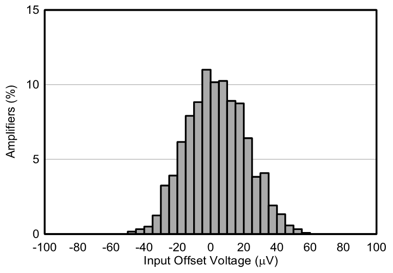
| N = 1225 | Mean = 3.63 μV | Std Dev = 18.0 μV |
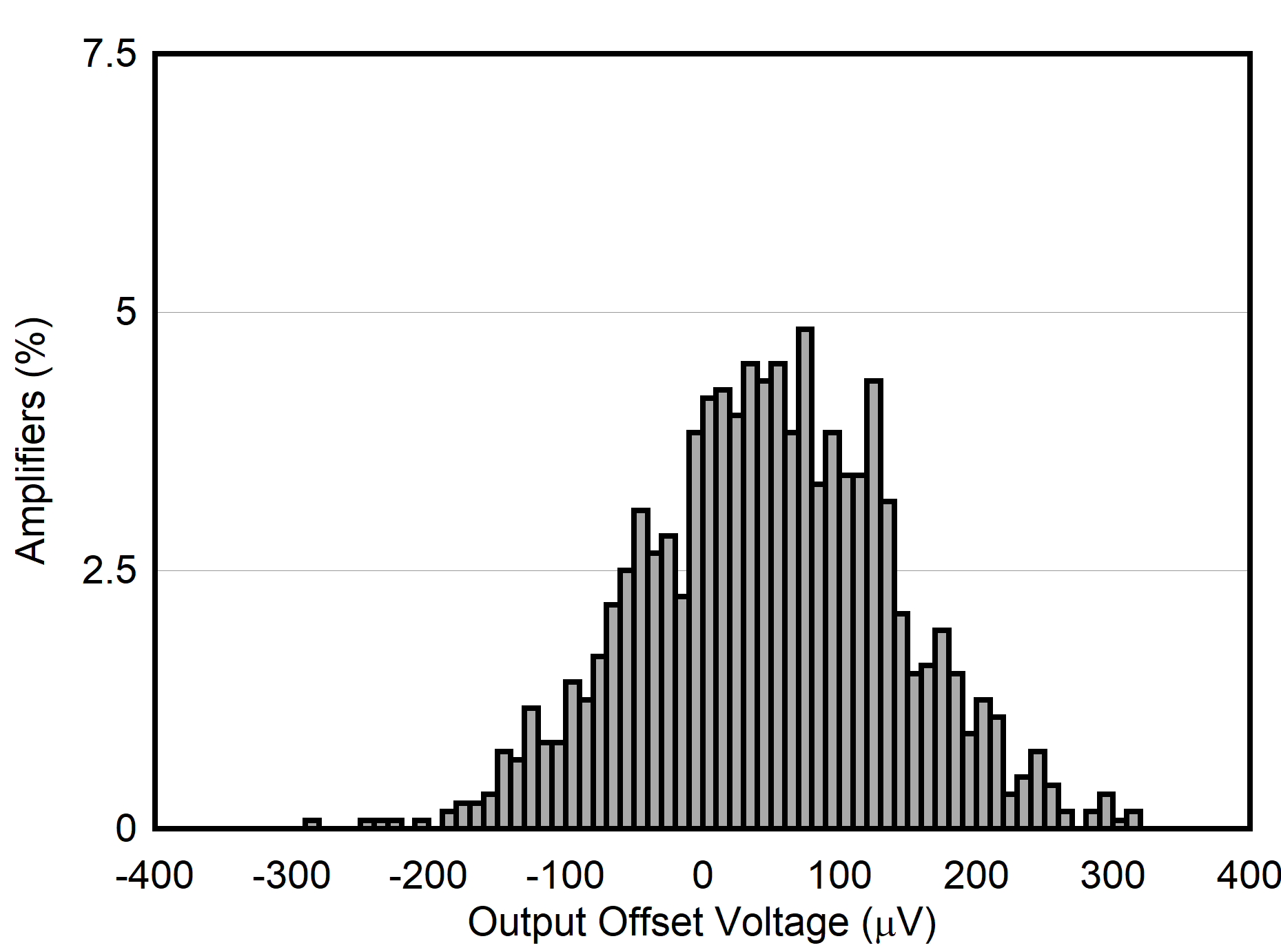
| N = 1225 | Mean = 48.0 μV | Std Dev = 92.4 μV |
| N = 1200 | Mean = 1.21 nA | Std Dev = 0.384 nA |
| N = 1170 | Mean = –0.092 nA | Std Dev = 0.35 nA |
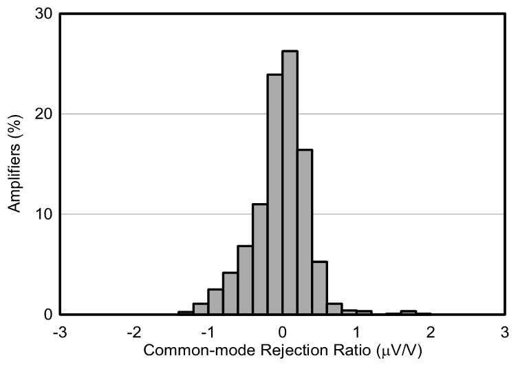
| N = 1225 | Mean = –0.0599 μV/V | Std. Dev = 0.710 μV/V |
| G = 10 |
| G = 1 |
| G = 1 | Average of 120 units | Normalized at +25°C |
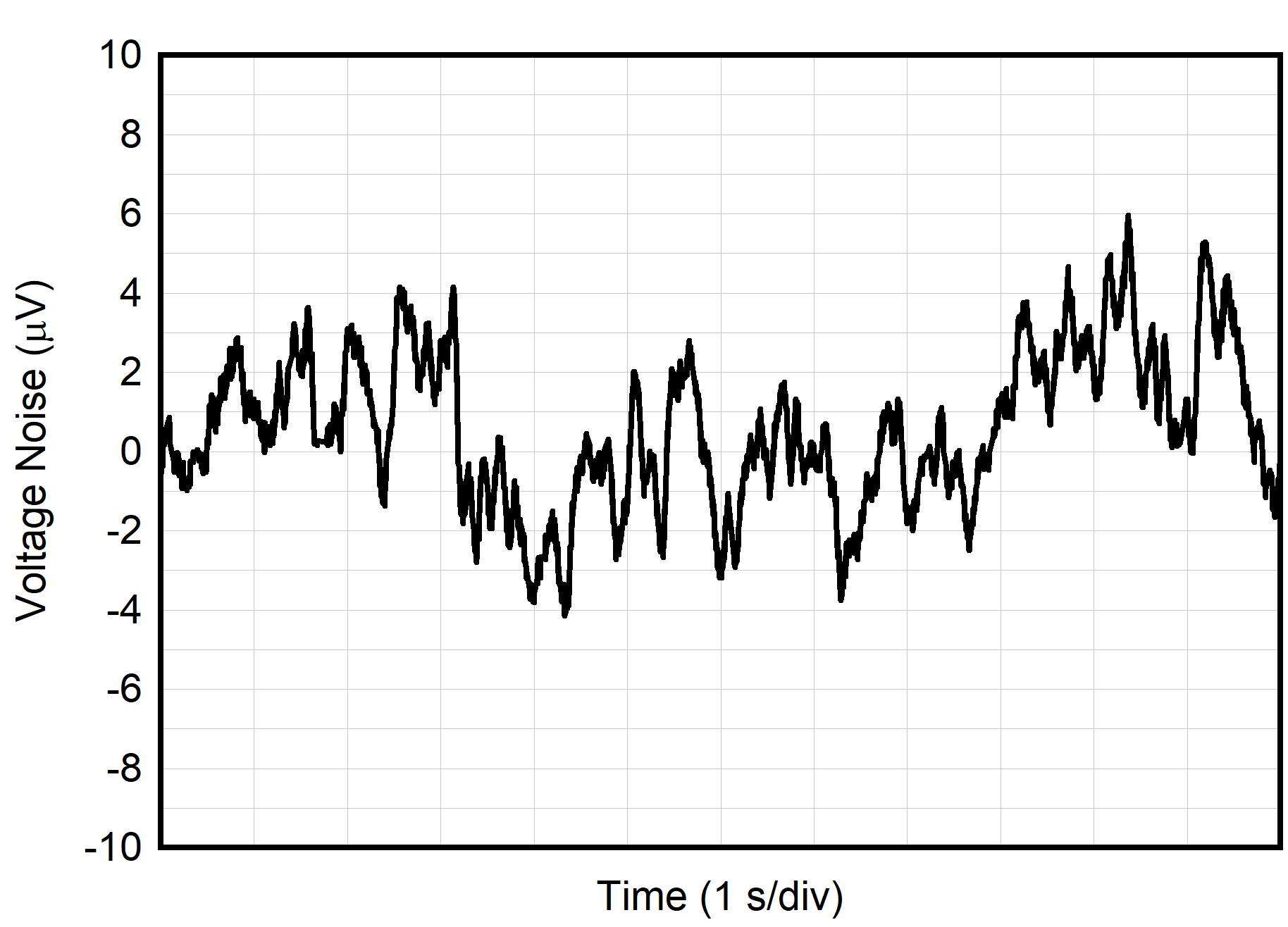
| G = 1 | RL = 10 kΩ | CL = 100 pF |
| G = 100 | RL = 10 kΩ | CL = 100 pF |
| VS = ±15 V |
| VS = ±15 V |
| VS = ±1.35 V |
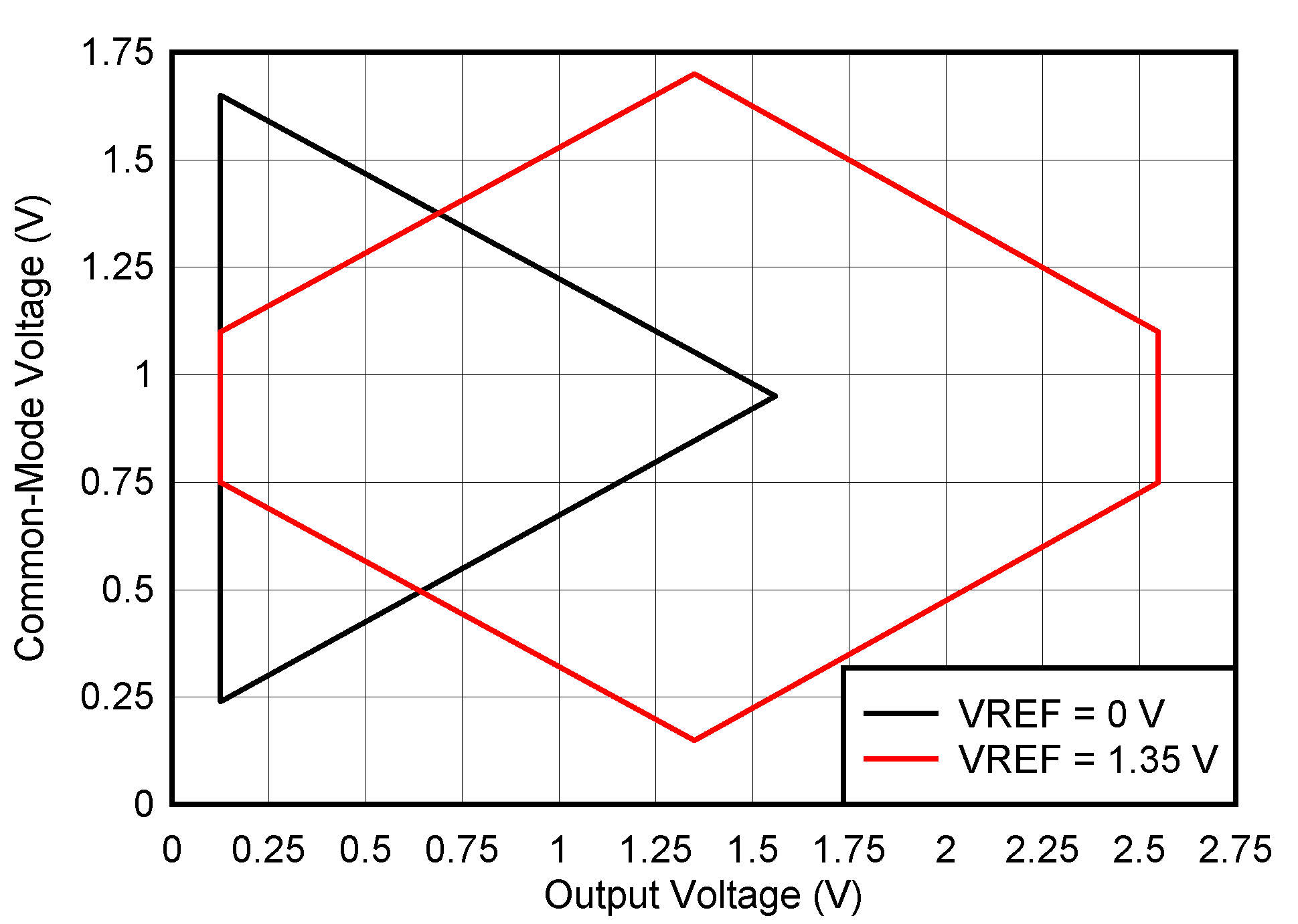
| VS = 2.7 V | G = 1 |
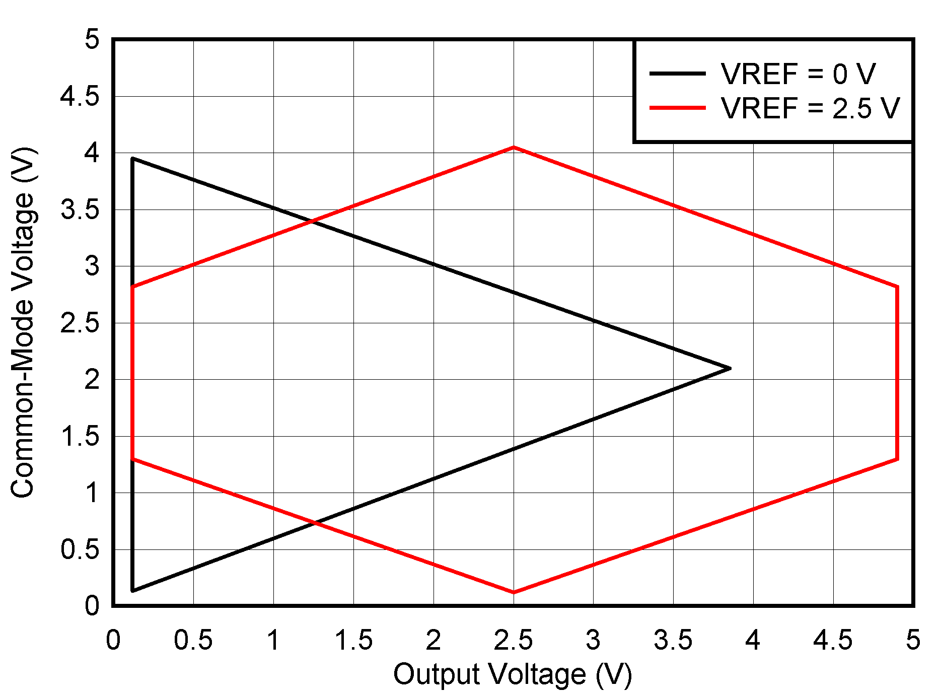
| VS = 5 V | G = 1 |
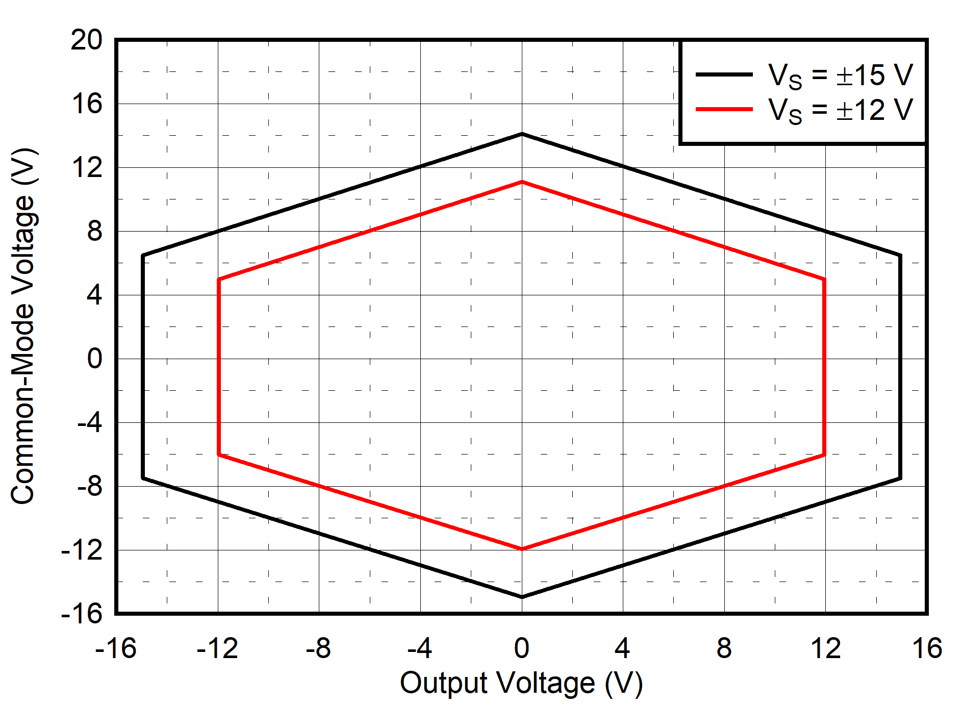
| G = 1 |
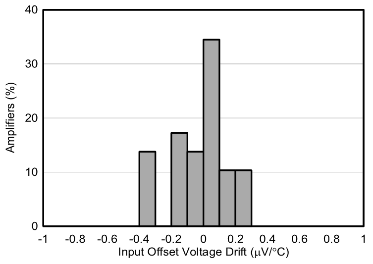
| N = 30 | Mean = –0.024 μV/ºC | Std Dev = 0.177 μV//ºC |
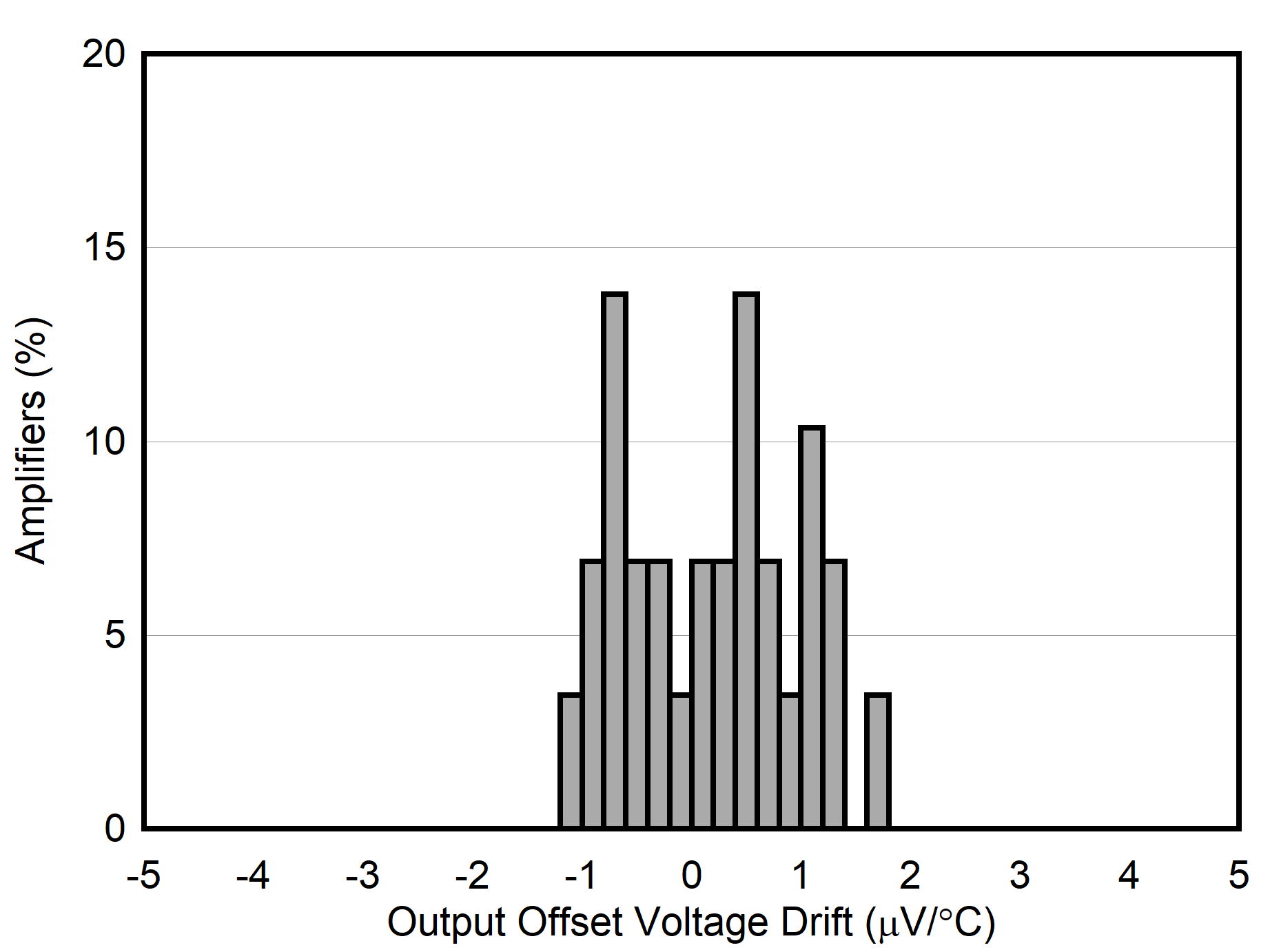
| N = 30 | Mean = 0.17 μV/ºC | Std Dev = 0.795 μV/ºC |
| N = 1200 | Mean = 1.11 nA | Std Dev = 0.368 nA |
| N = 1225 | Mean = –0.22 μV/V | Std Dev = 6.95 μV/V |
| N = 550 | Mean = –0.0334 % | Std. Dev = 0.0433 % |
| G = 10 |
| G = 10 |
| G = 100 | Average of 120 units | Normalized at +25°C |
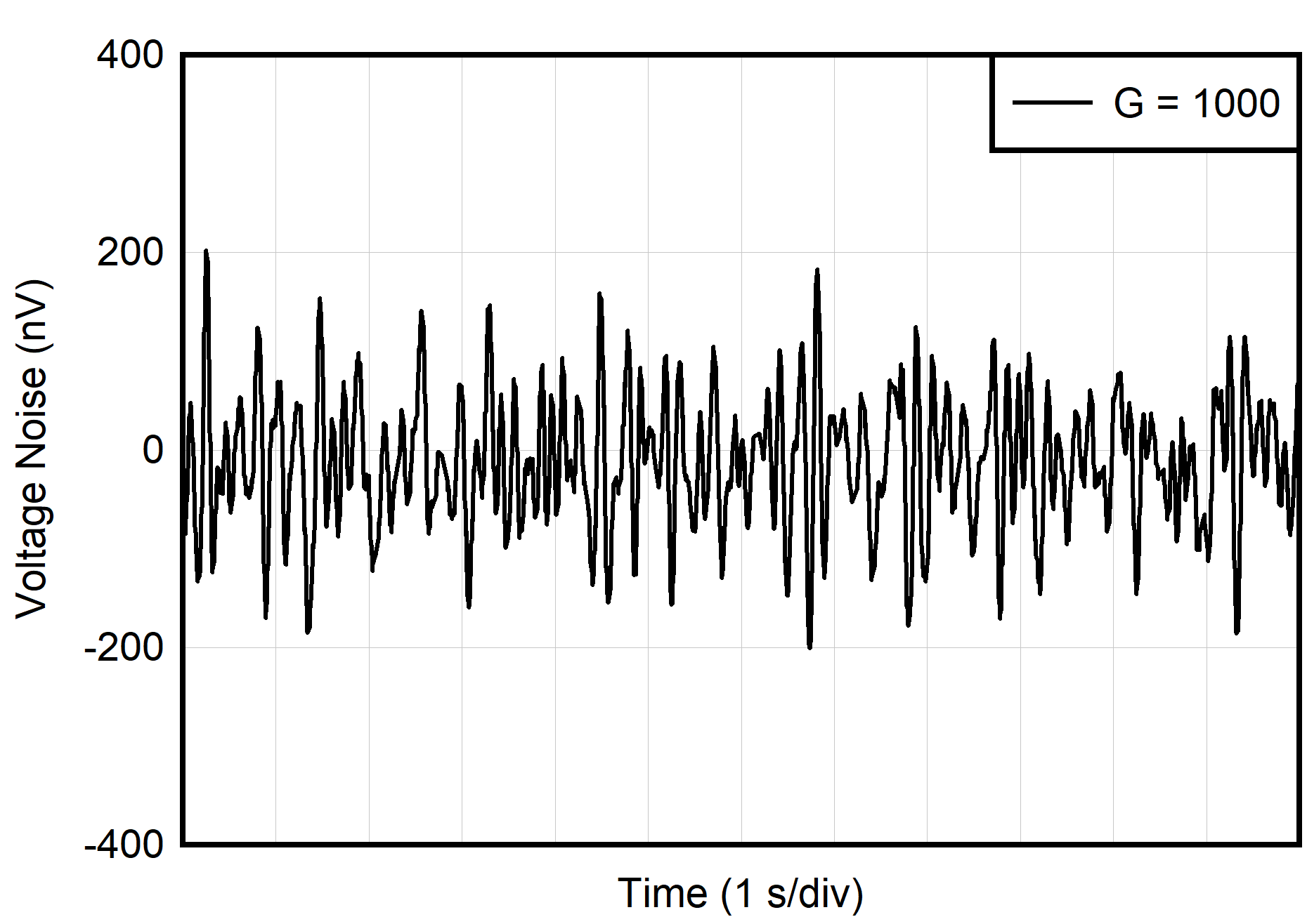
| G = 10 | RL = 10 kΩ | CL = 100 pF |
| G = 1000 | RL = 10 kΩ | CL = 100 pF |
| VS = ±15 V |
| VS = ±1.35 V |
| VS = ±15 V |
| VS = ±1.35 V |
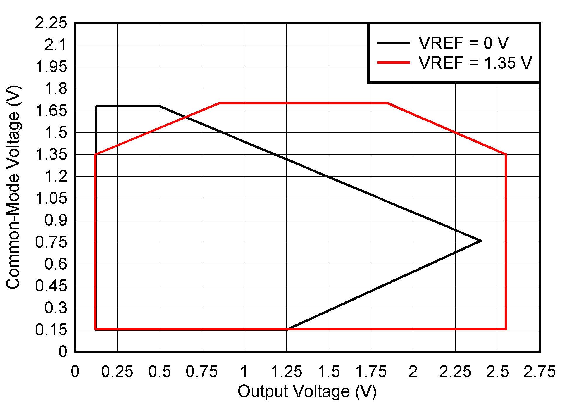
| VS = 2.7 V | G = 100 |
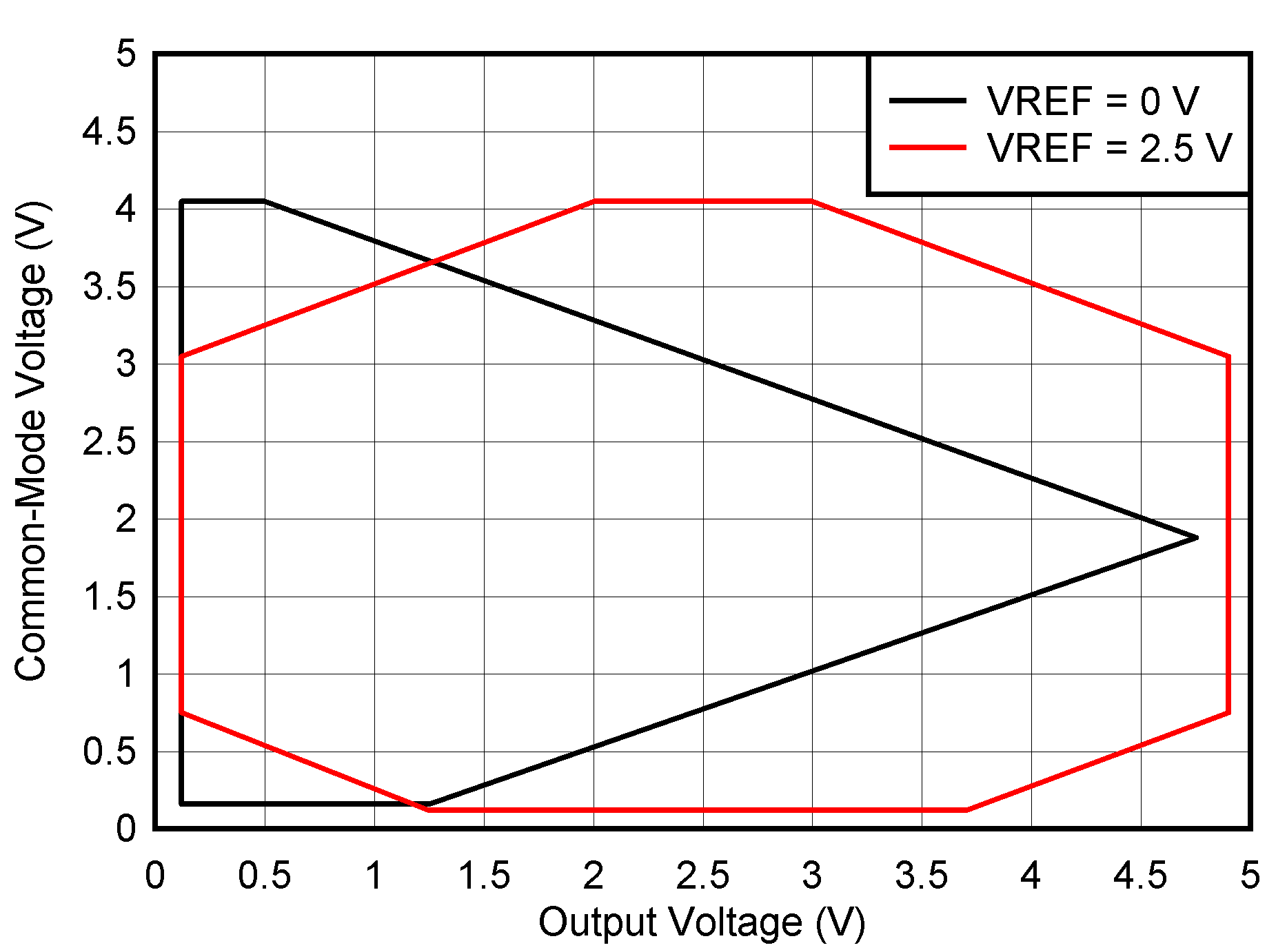
| VS = 5 V | G = 100 |
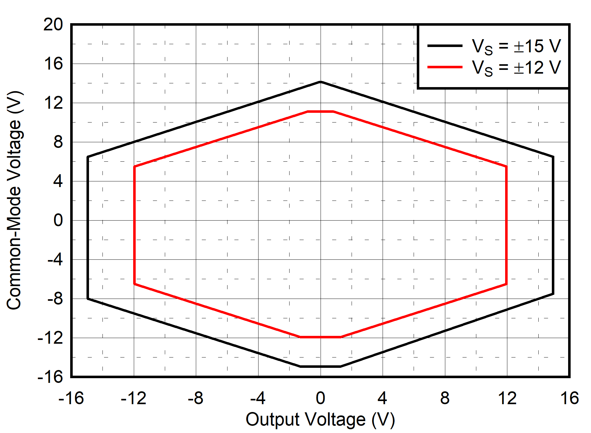
| G > 10 |