SLLSFU0C August 2023 – August 2025 ISO6520 , ISO6521
PRODUCTION DATA
- 1
- 1 Features
- 2 Applications
- 3 Description
- 4 Pin Configuration and Functions
-
5 Specifications
- 5.1 Absolute Maximum Ratings
- 5.2 ESD Ratings
- 5.3 Recommended Operating Conditions
- 5.4 Thermal Information
- 5.5 Package Characteristics
- 5.6 Electrical Characteristics—5-V Supply
- 5.7 Supply Current Characteristics—5-V Supply
- 5.8 Electrical Characteristics—3.3-V Supply
- 5.9 Supply Current Characteristics—3.3-V Supply
- 5.10 Electrical Characteristics—2.5-V Supply
- 5.11 Supply Current Characteristics—2.5-V Supply
- 5.12 Electrical Characteristics—1.8-V Supply
- 5.13 Supply Current Characteristics—1.8-V Supply
- 5.14 Switching Characteristics—5-V Supply
- 5.15 Switching Characteristics—3.3-V Supply
- 5.16 Switching Characteristics—2.5-V Supply
- 5.17 Switching Characteristics—1.8-V Supply
- 5.18 Typical Characteristics
- 6 Parameter Measurement Information
- 7 Detailed Description
- 8 Application and Implementation
- 9 Device and Documentation Support
- 10Revision History
- 11Mechanical, Packaging, and Orderable Information
Package Options
Mechanical Data (Package|Pins)
Thermal pad, mechanical data (Package|Pins)
Orderable Information
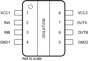
4 Pin Configuration and Functions
 Figure 4-1 ISO6520 D Package 8-Pin
SOIC Top View
Figure 4-1 ISO6520 D Package 8-Pin
SOIC Top ViewFigure 4-3 ISO6520 DFN Package 8-Pin REU Top View
 Figure 4-2 ISO6521 D Package 8-Pin
SOIC Top View
Figure 4-2 ISO6521 D Package 8-Pin
SOIC Top ViewFigure 4-4 ISO6521 DFN Package 8-Pin REU Top View
Table 4-1 Pin Functions
| NAME | PIN | TYPE(1) | Description | |
|---|---|---|---|---|
| ISO6520 | ISO6521 | |||
| GND1 | 4 | 4 | - | Ground connection for VCC1 |
| GND2 | 5 | 5 | - | Ground connection for VCC2 |
| INA | 2 | 7 | I | Input, channel A |
| INB | 3 | 3 | I | Input, channel B |
| OUTA | 7 | 2 | O | Output, channel A |
| OUTB | 6 | 6 | O | Output, channel B |
| VCC1 | 1 | 1 | P | Power supply, VCC1 |
| VCC2 | 8 | 8 | P | Power supply, VCC2 |
(1) I = Input, O = Output, P = Power