SLLSFC6D November 2021 – January 2023 ISOUSB111
PRODUCTION DATA
- 1 Features
- 2 Applications
- 3 Description
- 4 Revision History
- 5 Pin Configuration and Functions
-
6 Specifications
- 6.1 Absolute Maximum Ratings
- 6.2 ESD Ratings
- 6.3 Recommended Operating Conditions
- 6.4 Thermal Information
- 6.5 Power Ratings
- 6.6 Insulation Specifications
- 6.7 Safety-Related Certifications
- 6.8 Safety Limiting Values
- 6.9 Electrical Characteristics
- 6.10 Switching Characteristics
- 6.11 Insulation Characteristics Curves
- 6.12 Typical Characteristics
- 7 Parameter Measurement Information
-
8 Detailed Description
- 8.1 Overview
- 8.2 Functional Block Diagram
- 8.3
Feature Description
- 8.3.1 Power Supply Options
- 8.3.2 Power Up
- 8.3.3 Symmetric Operation, Dual-Role Port and Role-Reversal
- 8.3.4 Connect and Speed Detection
- 8.3.5 Disconnect Detection
- 8.3.6 Reset
- 8.3.7 LS/FS Message Traffic
- 8.3.8 L2 Power Management State (Suspend) and Resume
- 8.3.9 L1 Power Management State (Sleep) and Resume
- 8.4 Device Functional Modes
- 9 Power Supply Recommendations
- 10Application and Implementation
- 11Layout
- 12Device and Documentation Support
- 13Mechanical, Packaging, and Orderable Information
Package Options
Mechanical Data (Package|Pins)
- DWX|16
- DW|16
Thermal pad, mechanical data (Package|Pins)
Orderable Information
8.2 Functional Block Diagram
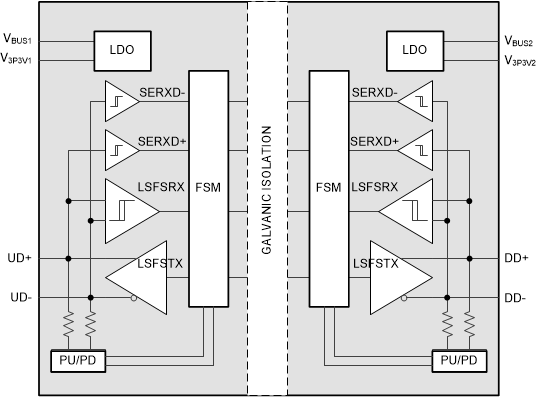
A simplified functional block diagram of ISOUSB111 is shown in Figure 8-1. The device comprises the following:
 Figure 8-1 ISOUSB111 Simplified
Functional Block Diagram.
- Transmit and receive circuits and pull-up and pull-down resistors according to the USB standard.
- Digital logic to handle bi-directional communication, and various state-transitions.
- Internal LDOs to generate V3P3Vx supplies from the VBUSx supplies.
- Galvanic isolation.
 Figure 8-1 ISOUSB111 Simplified
Functional Block Diagram.