SLRS008D September 1986 – January 2016 L293 , L293D
PRODUCTION DATA.
- 1 Features
- 2 Applications
- 3 Description
- 4 Revision History
- 5 Pin Configuration and Functions
- 6 Specifications
- 7 Parameter Measurement Information
- 8 Detailed Description
- 9 Application and Implementation
- 10Power Supply Recommendations
- 11Layout
- 12Device and Documentation Support
- 13Mechanical, Packaging, and Orderable Information
Package Options
Mechanical Data (Package|Pins)
- NE|16
Thermal pad, mechanical data (Package|Pins)
Orderable Information
8 Detailed Description
8.1 Overview
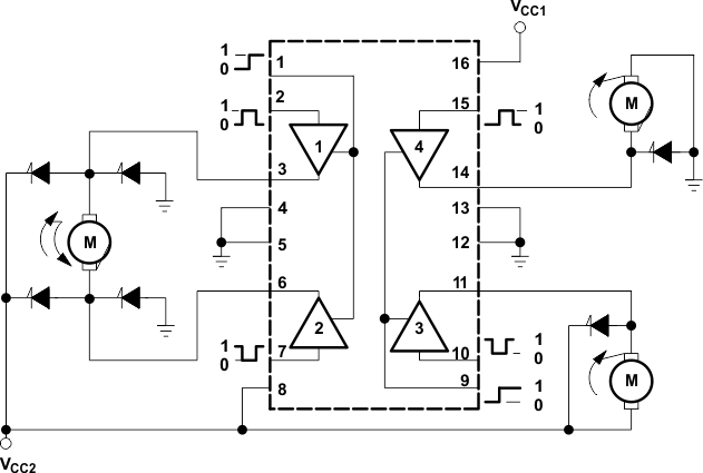
The L293 and L293D are quadruple high-current half-H drivers. These devices are designed to drive a wide array of inductive loads such as relays, solenoids, DC and bipolar stepping motors, as well as other high-current and high-voltage loads. All inputs are TTL compatible and tolerant up to 7 V.
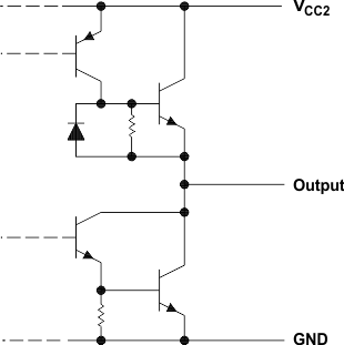
Each output is a complete totem-pole drive circuit, with a Darlington transistor sink and a pseudo-Darlington source. Drivers are enabled in pairs, with drivers 1 and 2 enabled by 1,2EN and drivers 3 and 4 enabled by 3,4EN. When an enable input is high, the associated drivers are enabled, and their outputs are active and in phase with their inputs. When the enable input is low, those drivers are disabled, and their outputs are off and in the high-impedance state. With the proper data inputs, each pair of drivers forms a full-H (or bridge) reversible drive suitable for solenoid or motor applications.
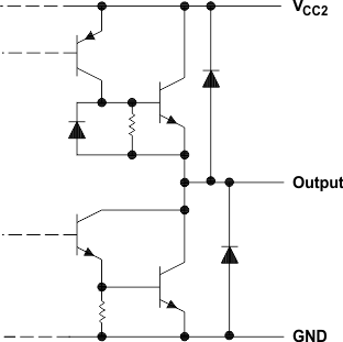
On the L293, external high-speed output clamp diodes should be used for inductive transient suppression. On the L293D, these diodes are integrated to reduce system complexity and overall system size. A VCC1 terminal, separate from VCC2, is provided for the logic inputs to minimize device power dissipation. The L293 and L293D are characterized for operation from 0°C to 70°C.
8.2 Functional Block Diagram

8.3 Feature Description
The L293x has TTL-compatible inputs and high voltage outputs for inductive load driving. Current outputs can get up to 2 A using the L293.
8.4 Device Functional Modes
Table 1 lists the fuctional modes of the L293x.
Table 1. Function Table (Each Driver)(1)
| INPUTS (2) | OUTPUT (Y) | |
|---|---|---|
| A | EN | |
| H | H | H |
| L | H | L |
| X | L | Z |
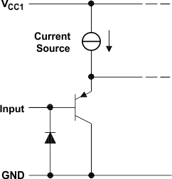
 Figure 3. Schematic of Inputs for the L293x
 Figure 4. Schematic of Outputs for the L293
 Figure 5. Schematic of Outputs for the L293D