SLRS008D September 1986 – January 2016 L293 , L293D
PRODUCTION DATA.
- 1 Features
- 2 Applications
- 3 Description
- 4 Revision History
- 5 Pin Configuration and Functions
- 6 Specifications
- 7 Parameter Measurement Information
- 8 Detailed Description
- 9 Application and Implementation
- 10Power Supply Recommendations
- 11Layout
- 12Device and Documentation Support
- 13Mechanical, Packaging, and Orderable Information
Package Options
Mechanical Data (Package|Pins)
- NE|16
Thermal pad, mechanical data (Package|Pins)
Orderable Information
10 Power Supply Recommendations
VCC1 is 5 V ± 0.5 V and VCC2 can be same supply as VCC1 or a higher voltage supply with peak voltage up to 36 V. Bypass capacitors of 0.1 uF or greater should be used at VCC1 and VCC2 pins. There are no power up or power down supply sequence order requirements.
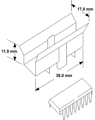
Properly heatsinking the L293 when driving high-current is critical to design. The Rthj-amp of the L293 can be reduced by soldering the GND pins to a suitable copper area of the printed circuit board or to an external heat sink.
Figure 14 shows the maximum package power PTOT and the θJA as a function of the side of two equal square copper areas having a thickness of 35 μm (see Figure 14). In addition, an external heat sink can be used (see Figure 12).
During soldering, the pin temperature must not exceed 260°C, and the soldering time must not exceed 12 seconds.
The external heatsink or printed circuit copper area must be connected to electrical ground.
 Figure 12. External Heat Sink Mounting Example (θJA = 25°C/W)