SNOSCY0 March 2014 LDC1051
PRODUCTION DATA.
- 1 Features
- 2 Applications
- 3 Description
- 4 Revision History
- 5 Terminal Configuration and Functions
- 6 Specifications
- 7 Detailed Description
- 8 Applications and Implementation
- 9 Power Supply Recommendations
- 10Layout
- 11Device and Documentation Support
- 12Mechanical, Packaging, and Orderable Information
Package Options
Mechanical Data (Package|Pins)
- NHR|16
Thermal pad, mechanical data (Package|Pins)
Orderable Information
8 Applications and Implementation
8.1 Application Information
8.1.1 Calculation of Rp_MIN and Rp_MAX
Different sensing applications may have a different range of the resonance impedance Rp to measure. The LDC1051 measurement range of Rp is controlled by setting 2 registers – Rp_MIN and Rp_MAX. For a given application, Rp must never be outside the range set by these register values, otherwise the measured value will be clipped. For optimal sensor resolution, the range of Rp_MIN to Rp_MAX should not be unnecessarily large. The following procedure is recommended to determine the Rp_MIN and Rp_MAX register values.
8.1.1.1 Setting Rp_MAX
Rp_MAX sets the upper limit of the LDC1051 resonant impedance input range.
- Configure the sensor such that the eddy current losses are minimized. As an example, for a proximity sensing application, set the distance between the sensor and the target to the maximum sensing distance.
- Measure the resonant impedance Rp using an impedance analyzer.
- Multiply Rp by 2 and use the next higher value from Table 4.
Note that setting Rp_MAX to a value not listed in Table 4 can result in indeterminate behavior.
8.1.1.2 Setting Rp_MIN
Rp_MIN sets the lower limit of the LDC1051 resonant impedance input range.
- Configure the sensor such that the eddy current losses are maximized. As an example, for a proximity sensing application, set the distance between the sensor and the metal target to the minimum sensing distance.
- Measure the resonant impedance Rp using an impedance analyzer.
- Divide the Rp value by 2 and then select the next lower Rp value from Table 6.
Note that setting Rp_MIN to a value not listed on Table 6 can result in indeterminate behavior. In addition, Rp_MIN powers on with a default value of 0x14 which must be set to a value from Table 6 prior to powering on the LDC.
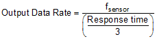
8.1.2 Output Data Rate
Output data rate of LDC1051 depends on the sensor frequency, fsensor and 'Response Time' field in LDC Configuration register(Address:0x04).
8.1.3 Choosing Filter Capacitor (CFA and CFB Terminals)
The Filter capacitor is critical to the operation of the LDC1051. The capacitor should be low leakage, temperature stable, and it must not generate any piezoelectric noise (the dielectrics of many capacitors exhibit piezoelectric characteristics and any such noise is coupled directly through Rp into the converter). The optimal capacitance values range from 20pF to 100nF. The value of the capacitor is based on the time constant and resonating frequency of the LC tank.
If a ceramic capacitor is used, then a C0G (or NP0) grade dielectric is recommended; the voltage rating should be ≥10V. The traces connecting CFA and CFB to the capacitor should be as short as possible to minimize any parasitics.
For optimal performance, the chosen filter capacitor, connected between terminals CFA and CFB, needs to be as small as possible, but large enough such that the active filter does not saturate. The size of this capacitor depends on the time constant of the sense coil, which is given by L/Rs, (L=inductance, Rs=series resistance of the inductor at oscillation frequency). The larger this time constant, the larger filter capacitor is required. Hence, this time constant reaches its maximum when there is no target present in front of the sensing coil.
The following procedure can be used to find the optimal filter capacitance:
- Start with a large filter capacitor. For a ferrite core coil, 10nF is usually large enough. For an air coil or PCB coil, 100pF is usually large enough.
- Power on the LDC and set the desired register values. Minimize the eddy currents losses. This is done by minimizing the amount of conductive target covering the sensor. For an axial sensing application, the target should be at farthest distance from coil. For a lateral or angular position sensing application, the target coverage of the coil should be minimized.
- Observe the signal on the CFB terminal using a scope. Since this node is very sensitive to capacitive loading, it is recommended to use an active probe. As an alternative, a passive probe with a 1kΩ series resistance between the tip and the CFB terminal can be used.
- Vary the values of the filter capacitor until that the signal observed on the CFB terminal has an amplitude of approximate 1V peak-to-peak. This signal scales linearly with the reciprocal of the filter capacitance. For example, if a 100pF filter capacitor is applied and the signal observed on the CFB terminal has a peak-to-peak value of 200mV, the desired 1V peak-to-peak value is obtained using a 200mV / 1V * 100pF = 20pF filter capacitor.
8.2 Typical Applications
8.2.1 Axial Distance Sensing Using a PCB Sensor with LDC1051
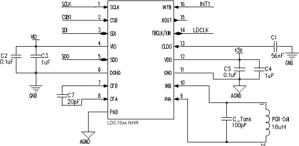 Figure 16. Typical Application Schematic, LDC10xx
8.2.1.1 Design Requirements
For this design example, use the following as the input parameters.
Table 15. Design Parameters
| DESIGN PARAMETER | EXAMPLE VALUE |
|---|---|
| Minimum sensing distance | 1 mm |
| Maximum sensing distance | 8 mm |
| Output data rate | 78 KSPS (Max data rate with LDC10xx series) |
| Number of PCB layers for sensor | 2 layers |
8.2.1.2 Detailed Design Procedure
8.2.1.2.1 Sensor and Target
In this example, consider a sensor with the below characteristics.
Table 16. Sensor Characteristics
| PARAMETER | VALUE |
|---|---|
| Layers | 2 |
| Thickness of copper | 1 Oz |
| Coil shape | Circular |
| Number of turns | 23 |
| Trace thickness | 4 mil |
| Trace spacing | 4 mil |
| PCB core material | FR4 |
| Rp @ 1 mm | 5 kΩ |
| Rp @ 8 mm | 12.5 kΩ |
| Nominal Inductance | 18 µH |
Target material used is stainless steel
8.2.1.2.2 Calculating Sensor Capacitor
Sensor frequency depends on various factors in the application. In this example since one of the design parameter is to achieve output data rate of 78 KSPS, sensor frequency can be calculated as below.
With the lowest Response time of 192 and output data rate of 78 KSPS, sensor frequency calculated using the above formula is 4.99 MHz.
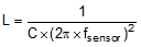
Now, using the below formula sensor capacitor is calculated to be 55 pF with a sensor inductance of 18 µH
8.2.1.2.3 Choosing Filter Capacitor
Using the steps given in Choosing Filter Capacitor (CFA and CFB Terminals) filter capacitor for the example sensor is 20 pF. Below waveform shows the pattern on CFB terminal with 100 pF and 20 pF filter capacitor.
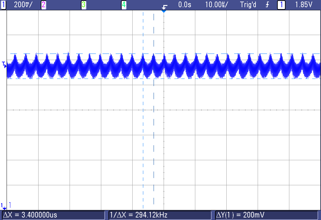 Figure 17. Waveform On CFB With 100pf
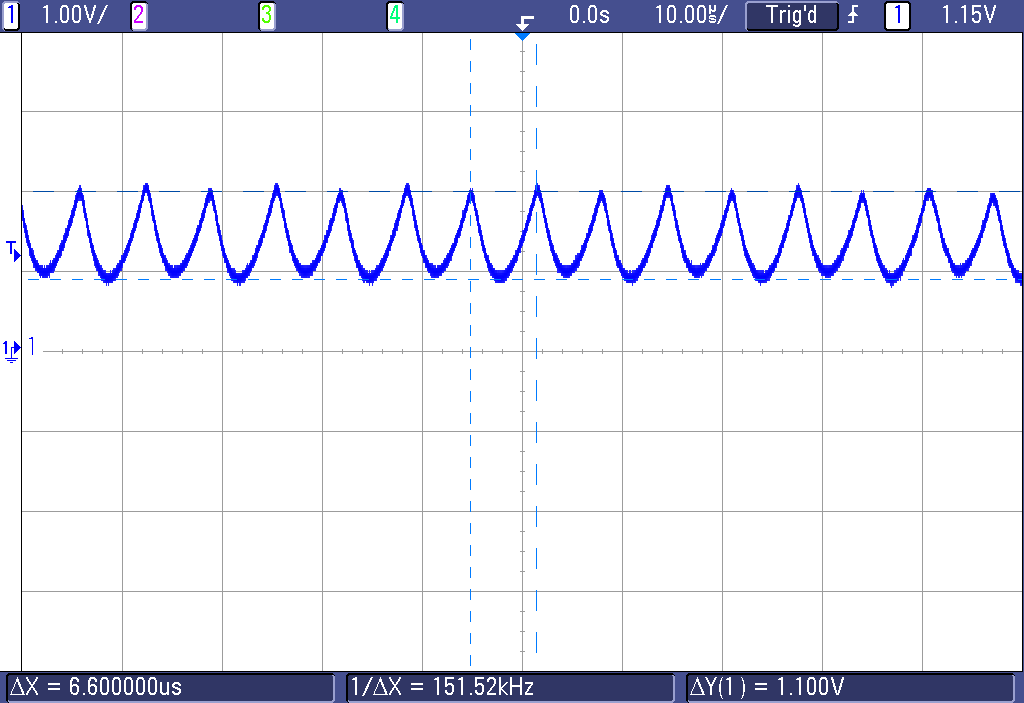 Figure 18. Waveform On CFB With 20pf
8.2.1.2.4 Setting Rp_MIN and Rp_MAX
Calculating value for Rp_MAX Register : Rp at 8mm is 12.5kΩ, 12500×2 = 25000. In Table 4, then 27.704 kΩ is the nearest value larger than 25kΩ; this corresponds to Rp_MAX value of 0x12
Calculating value for Rp_MIN Register : Rp at 1mm is 5kΩ, 5000/2 = 2500. In Table 6, 2.394kΩ is the nearest value lower than 2.5kΩ; this corresponds to Rp_MIN value of 0x3B
8.2.1.2.5 Calculating Minimum Sensor Frequency
Using,
N is 227.51, round off to 228 decimal. This value has to be written into Watchdog Timer Register, which is used to wake up the internal circuit when the sensor is saturated.
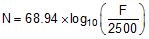
8.2.1.3 Application Curves
 Figure 19. Rp vs Distance
8.2.2 Lateral Position Sensing Application Diagram
 Figure 20. Linear Position Sensing
8.2.3 Angular Position Sensing Application Diagram
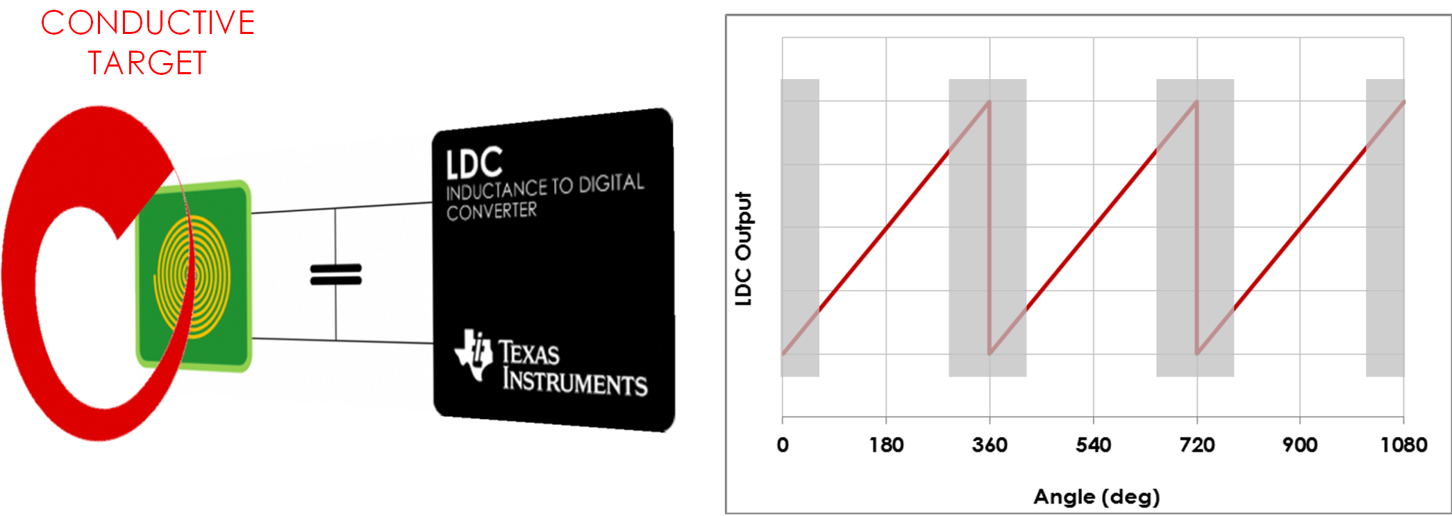 Figure 21. Angular Position Sensing