SNOSCY0 March 2014 LDC1051
PRODUCTION DATA.
- 1 Features
- 2 Applications
- 3 Description
- 4 Revision History
- 5 Terminal Configuration and Functions
- 6 Specifications
- 7 Detailed Description
- 8 Applications and Implementation
- 9 Power Supply Recommendations
- 10Layout
- 11Device and Documentation Support
- 12Mechanical, Packaging, and Orderable Information
Package Options
Mechanical Data (Package|Pins)
- NHR|16
Thermal pad, mechanical data (Package|Pins)
Orderable Information
6 Specifications
6.1 Absolute Maximum Ratings
| MIN | MAX | UNIT | ||
|---|---|---|---|---|
| Analog Supply Voltage (VDD – GND) | 6 | V | ||
| IO Supply Voltage (VIO – GND) | 6 | V | ||
| Voltage on any Analog Terminal | –0.3 | VDD + 0.3 | V | |
| Voltage on any Digital Terminal | –0.3 | VIO + 0.3 | V | |
| Input Current on INA and INB | 8 | mA | ||
| Junction Temperature, TJ | 150 | °C | ||
6.2 Handling Ratings
| MIN | MAX | UNIT | ||
|---|---|---|---|---|
| Tstg | Storage Temperature range | -65 | 150 | °C |
| VESD | Human Body Model (HBM) ESD stress voltage | 1k | 1k | V |
| Charge Device Model (CDM) ESD stress voltage | 250 | 250 | V |
6.3 Recommended Operating Conditions
over operating free-air temperature range (unless otherwise noted)| MIN | MAX | UNIT | ||
|---|---|---|---|---|
| Analog Supply Voltage (VDD – GND) | 4.75 | 5.25 | V | |
| IO Supply Voltage (VIO – GND) | 1.8 | 5.25 | V | |
| VDD-VIO | 0 | V | ||
| Operating Temperature, TA | -40 | 125 | °C | |
6.4 Thermal Information
| THERMAL METRIC(1) | NHR (16-TERMINALS) |
UNIT | |
|---|---|---|---|
| θJA | Junction-to-ambient thermal resistance | 28 | °C/W |
(1) For more information about traditional and new thermal metrics, see the IC Package Thermal Metrics application report, SPRA953.
6.5 Electrical Characteristics(1)
Unless otherwise specified, all limits ensured for TA = TJ = 25°C, VDD = 5 V, VIO = 3.3 V| PARAMETER | TEST CONDITIONS | MIN(3) | TYP(2) | MAX(3) | UNIT | |
|---|---|---|---|---|---|---|
| POWER | ||||||
| VDD | Analog supply voltage | 4.75 | 5 | 5.25 | V | |
| VIO | IO supply voltage | VIO≤VDD | 1.8 | 3.3 | 5.25 | V |
| IDD | Supply current, VDD | Does not include sensor current.(4) | 1.7 | 2.3 | mA | |
| IVIO | IO supply current | Static current | 14 | µA | ||
| IDD_LP | Stand-by mode supply current | 250 | µA | |||
| tSTART | Start-Up Time | From POR to ready-to-convert. | 2 | ms | ||
| LDC | ||||||
| ƒsensor_MIN | Minimum sensor frequency | 5 | kHz | |||
| ƒsensor_MAX | Maximum sensor frequency | 5 | MHz | |||
| Asensor_MIN | Minimum sensor amplitude | 1 | VPP | |||
| Asensor_MAX | Maximum sensor amplitude | 4 | VPP | |||
| tREC | Recovery time | Oscillation start-up time after Rp under-range condition | 10 | 1/fsensor | ||
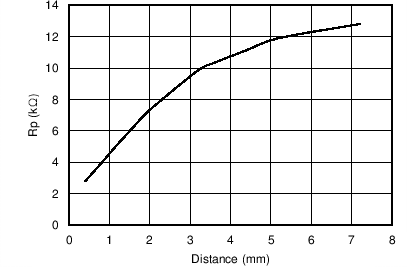
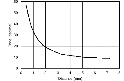
| Rp Min | Minimum sensor Rp range | 798 | Ω | |||
| Rp Max | Maximum Sensor Rp range | 3.93 | MΩ | |||
| Rp Res | Rp measurement resolution | 8 | Bits | |||
| tS_MIN | Minimum response time | Minimum programmable settling time of digital filter | 192 × 1 / ƒsensor | s | ||
| tS_MAX | Maximum response time | Maximum programmable settling time of digital filter | 6144 × 1 / ƒsensor | s | ||
| DIGITAL I/O CHARACTERISTICS | ||||||
| VIH | Logic 1 input voltage | 0.8 × VIO | V | |||
| VIL | Logic 0 input voltage | 0.2 × VIO | V | |||
| VOH | Logic 1 output voltage | ISOURCE = 400 µA | VIO – 0.3 | V | ||
| VOL | Logic 0 output voltage | ISINK = 400 µA | 0.3 | V | ||
| IIOHL | Digital IO leakage current | –500 | 500 | nA | ||
(1) Electrical Characteristics Table values apply only for factory testing conditions at the temperature indicated. Factory testing conditions result in very limited self-heating of the device such that TJ = TA. No specification of parametric performance is indicated in the electrical tables under conditions of internal self-heating where TJ > TA. Absolute Maximum Ratings indicate junction temperature limits beyond which the device may be permanently degraded, either mechanically or electrically.
(2) Typical values represent the most likely parametric norm as determined at the time of characterization. Actual typical values may vary over time and will also depend on the application and configuration. The typical values are not tested and are not specified on shipped production material.
(3) Limits are specified by testing, design, or statistical analysis at 25°C. Limits over the operating temperature range are specified through correlations using statistical quality control (SQC) method.
(4) LC tank current depends on the Q-factor of the tank, distance and material of the target.
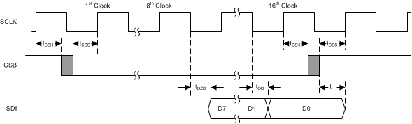
6.6 Timing Requirements
Unless otherwise noted, all limits specified at TA = 25°C, VDD = 5, VIO = 3.3, 10 pF capacitive load in parallel with a 10 kΩ load on the SDO terminal. Specified by design; not production tested.| PARAMETER | MIN | TYP | MAX | UNIT | ||
|---|---|---|---|---|---|---|
| ƒSCLK | Serial Clock Frequency | 4 | MHz | |||
| tPH | SCLK Pulse Width High | ƒSCLK = 4 MHz | 0.4 / ƒSCLK | s | ||
| tPL | SCLK Pulse Width Low | ƒSCLK = 4 MHz | 0.4 / ƒSCLK | s | ||
| tSU | SDI Setup Time | 10 | ns | |||
| tH | SDI Hold Time | 10 | ns | |||
| tODZ | SDO Driven-to-Tristate Time | Measured at 10% / 90% point | 20 | ns | ||
| tOZD | SDO Tristate-to-Driven Time | Measured at 10% / 90% point | 20 | ns | ||
| tOD | SDO Output Delay Time | 20 | ns | |||
| tCSS | CSB Setup Time | 20 | ns | |||
| tCSH | CSB Hold Time | 20 | ns | |||
| tIAG | Inter-Access Gap | 100 | ns | |||
| tDRDYB | Data ready pulse width | Data ready pulse at every 1 / ODR if no data is read | 1 / ƒsensor | s | ||
Unless otherwise noted, all limits specified at TA = 25°C, VDD=5.0, VIO=3.3, 10pF capacitive load in parallel with a 10kΩ load on SDO. Specified by design; not production tested.
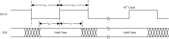 Figure 1. Write Timing Diagram