SNOSCZ0A December 2014 – March 2018 LDC1312 , LDC1314
PRODUCTION DATA.
- 1 Features
- 2 Applications
- 3 Description
- 4 Revision History
- 5 Pin Configuration and Functions
- 6 Specifications
-
7 Detailed Description
- 7.1 Overview
- 7.2 Functional Block Diagram
- 7.3 Feature Description
- 7.4 Device Functional Modes
- 7.5 Programming
- 7.6
Register Maps
- 7.6.1 Register List
- 7.6.2 Address 0x00, DATA0
- 7.6.3 Address 0x02, DATA1
- 7.6.4 Address 0x04, DATA2 (LDC1314 only)
- 7.6.5 Address 0x06, DATA3 (LDC1314 only)
- 7.6.6 Address 0x08, RCOUNT0
- 7.6.7 Address 0x09, RCOUNT1
- 7.6.8 Address 0x0A, RCOUNT2 (LDC1314 only)
- 7.6.9 Address 0x0B, RCOUNT3 (LDC1314 only)
- 7.6.10 Address 0x0C, OFFSET0
- 7.6.11 Address 0x0D, OFFSET1
- 7.6.12 Address 0x0E, OFFSET2 (LDC1314 only)
- 7.6.13 Address 0x0F, OFFSET3 (LDC1314 only)
- 7.6.14 Address 0x10, SETTLECOUNT0
- 7.6.15 Address 0x11, SETTLECOUNT1
- 7.6.16 Address 0x12, SETTLECOUNT2 (LDC1314 only)
- 7.6.17 Address 0x13, SETTLECOUNT3 (LDC1314 only)
- 7.6.18 Address 0x14, CLOCK_DIVIDERS0
- 7.6.19 Address 0x15, CLOCK_DIVIDERS1
- 7.6.20 Address 0x16, CLOCK_DIVIDERS2 (LDC1314 only)
- 7.6.21 Address 0x17, CLOCK_DIVIDERS3 (LDC1314 only)
- 7.6.22 Address 0x18, STATUS
- 7.6.23 Address 0x19, ERROR_CONFIG
- 7.6.24 Address 0x1A, CONFIG
- 7.6.25 Address 0x1B, MUX_CONFIG
- 7.6.26 Address 0x1C, RESET_DEV
- 7.6.27 Address 0x1E, DRIVE_CURRENT0
- 7.6.28 Address 0x1F, DRIVE_CURRENT1
- 7.6.29 Address 0x20, DRIVE_CURRENT2 (LDC1314 only)
- 7.6.30 Address 0x21, DRIVE_CURRENT3 (LDC1314 only)
- 7.6.31 Address 0x7E, MANUFACTURER_ID
- 7.6.32 Address 0x7F, DEVICE_ID
-
8 Application and Implementation
- 8.1
Application Information
- 8.1.1 Conductive Objects in a Time-Varying EM Field
- 8.1.2 L-C Resonators
- 8.1.3 Multi-Channel and Single Channel Operation
- 8.1.4 Sensor Conversion Time
- 8.1.5 Sensor Current Drive Configuration
- 8.1.6 Clocking Architecture
- 8.1.7 Input Deglitch Filter
- 8.1.8 Device Status Registers
- 8.1.9 Multi-Channel Data Readback
- 8.2 Typical Application
- 8.1
Application Information
- 9 Power Supply Recommendations
- 10Layout
- 11Device and Documentation Support
- 12Mechanical, Packaging, and Orderable Information
Package Options
Mechanical Data (Package|Pins)
- RGH|16
Thermal pad, mechanical data (Package|Pins)
Orderable Information
8.1.2 L-C Resonators
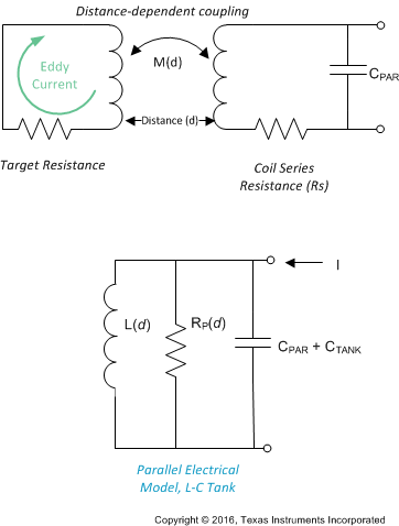
An EM field can be generated using an L-C resonator, or L-C tank. One topology for an L-C tank is a parallel R-L-C construction, as shown in Figure 46.
 Figure 46. Electrical Model of the L-C Tank Sensor
A resonant oscillator can be constructed by combining a frequency selective circuit (resonator) with a gain block in a closed loop. The criteria for oscillation are: (1) loop gain > 1, and (2) closed loop phase shift of 2π radians. The R-L-C resonator provides the frequency selectivity and contributes to the phase shift. At the resonance frequency, the impedance of the reactive components (L and C) cancels, leaving only RP, the lossy (resistive) element in the circuit. The voltage amplitude is maximized at this frequency. The RP can be used to determine the sensor drive current for a given oscillation amplitude. A lower RP requires a larger sensor current to maintain a constant oscillation amplitude. The sensor oscillation frequency is given by:

where
- C is the sensor capacitance (CSENSOR + CPARASITIC)
- L is the sensor inductance
The value of Q can be calculated by:

where
- RP is the AC parallel resistance of the LC resonator at the operating frequency
Texas Instruments' WEBENCH design tool can be used for coil design, in which the parameter values for RP, L and C are calculated. See http://www.ti.com/webench.
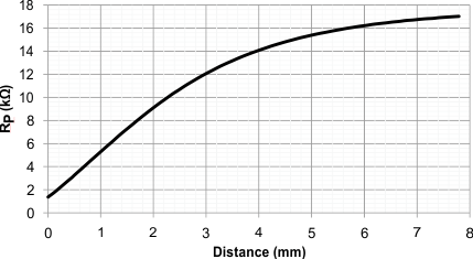
RP is a function of target distance, target material, and sensor characteristics. Figure 47 shows an example of RP variation based on the distance between the sensor and the target. The graph represents a 14 mm diameter PCB coil (23 turns, 4 mil trace width, 4 mil spacing between traces, 1 oz. copper thickness, on FR4 material). This curve is a typical response where the target distance scales based on the sensor size and the sensor RP scales based on the free-space of the inductor.
 Figure 47. Example RP vs. Distance with a 14 mm PCB Coil and 2 mm Thick Stainless Steel Target
It is important to configure the sensor current drive so that the sensor will still oscillate at the minimum RP value (which typically occurs with maximum target interaction). As an example, if the closest target distance in a system with the response shown in Figure 47 is 1mm, then the sensor current drive needs to support a RP value is 5 kΩ. Both the minimum and maximum RP conditions should have oscillation amplitudes that are within the device operating range. See section Sensor Current Drive Control for details on setting the current drive.
The inductance that is measured by the LDC is:

where
- L(d) is the measured sensor inductance, for a distance d between the sensor coil and target
- Linf is the inductance of the sensing coil without a conductive target (target at infinite distance)
- M(d) is the mutual inductance
- ƒSENSOR = sensor oscillation frequency for a distance d between the sensor coil and target
- C = CSENSOR + CPARASITIC
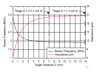
Figure 48 shows an example of variation in sensor frequency and inductance as a function of distance for a 14 mm diameter PCB coil (23 turns, 4 mil trace width, 4 mil spacing between traces, 1 oz copper thickness, FR4 material). The frequency and inductance graphs will scale based on the sensor free-space characteristics, and the target distance scales based on the sensor diameter.
 Figure 48. Example Sensor Frequency, Inductance vs. Target Distance
with 14 mm PCB Coil and 1.5 mm Thick Aluminum Target
The Texas Instruments Application Notes LDC Sensor Design and LDC Target Design provide more information on construction of sensors and targets charactersitics to consider based on system requirements.