SNVS778E May 1999 – January 2016 LM137 , LM337-N
PRODUCTION DATA.
- 1 Features
- 2 Applications
- 3 Description
- 4 Revision History
- 5 Pin Configuration and Functions
- 6 Specifications
- 7 Detailed Description
- 8 Application and Implementation
- 9 Power Supply Recommendations
- 10Layout
- 11Device and Documentation Support
- 12Mechanical, Packaging, and Orderable Information
Package Options
Mechanical Data (Package|Pins)
- NDT|3
Thermal pad, mechanical data (Package|Pins)
Orderable Information
8 Application and Implementation
NOTE
Information in the following applications sections is not part of the TI component specification, and TI does not warrant its accuracy or completeness. TI’s customers are responsible for determining suitability of components for their purposes. Customers should validate and test their design implementation to confirm system functionality.
8.1 Application Information
The LM137 and LM337-N are versatile, high performance, negative output linear regulators with high accuracy and a wide temperature range. An output capacitor can be added to further improve transient response, and the ADJ pin can be bypassed to achieve very high ripple-rejection ratios. The device's functionality can be utilized in many different applications that require negative voltage supplies, such as bipolar amplifiers, operational amplifiers, and constant current regulators.
8.2 Typical Applications
8.2.1 Adjustable Negative Voltage Regulator
The LM137 and LM337-N can be used as a simple, negative output regulator to enable a variety of output voltages needed for demanding applications. By using an adjustable R2 resistor, a variety of negative output voltages can be made possible as shown in Figure 16.
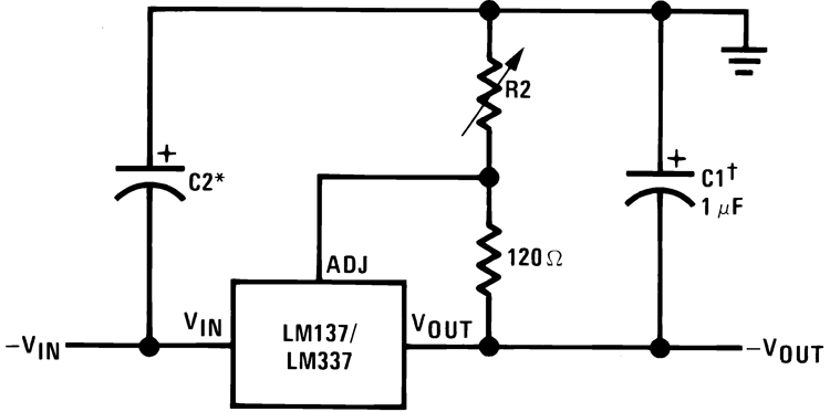
†C1 = 1-μF solid tantalum or 10-μF aluminum electrolytic required for stability
*C2 = 1-μF solid tantalum is required only if regulator is more than 4 inches from power-supply filter capacitor
Output capacitors in the range of 1 μF to 1000 μF of aluminum or tantalum electrolytic are commonly used to provide improved output impedance and rejection of transients

8.2.1.1 Design Requirements
The device component count is very minimal, employing two resistors as part of a voltage divider circuit and an output capacitor for load regulation. An input capacitor is needed if the device is more than 4 inches from the filter capacitors.
8.2.1.2 Detailed Design Procedure
The output voltage is set based on the selection of the two resistors, R1 and R2, as shown in Figure 16.
8.2.1.3 Application Curve
As shown in Figure 17, the maximum output current capability is limited by the input-output voltage differential, package type, and junction temperature.
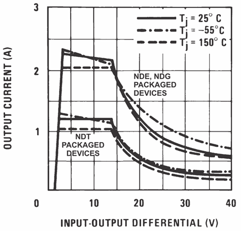 Figure 17. Current Limit
8.2.2 Adjustable Lab Voltage Regulator
The LM337-N can be combined with a positive regulator such as the LM317-N to provide both a positive and negative voltage rail. This can be useful in applications that use bi-directional amplifiers and dual-supply operational amplifiers.
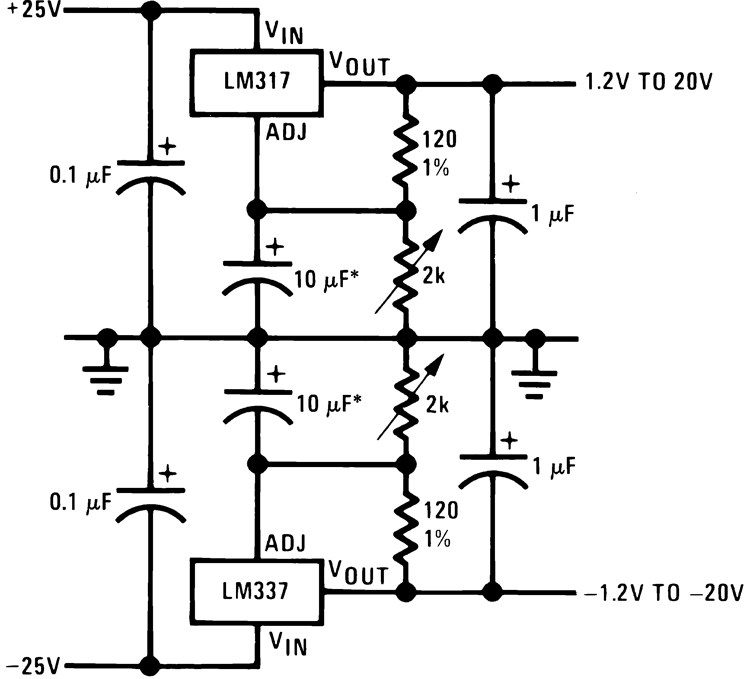
*The 10 μF capacitors are optional to improve ripple rejection
8.2.3 Current Regulator
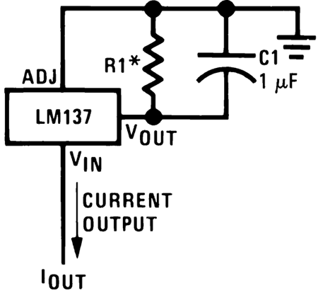
A simple, fixed current regulator can be made by placing a resistor between the VOUT and ADJ pins of the LM137. By regulating a constant 1.25 V between these two terminals, a constant current can be delivered.


8.2.4 −5.2-V Regulator with Electronic Shutdown
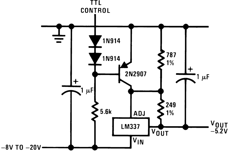
The LM337-N can be used with a PNP transistor to provide shutdown control from a TTL control signal. The PNP can short or open the ADJ pin to GND. When ADJ is shorted to GND by the PNP, the output is −1.3V. When ADJ is disconnected from GND by the PNP, then the LM337-N outputs the programmed output of −5.2 V.
8.2.5 High Stability −10-V Regulator
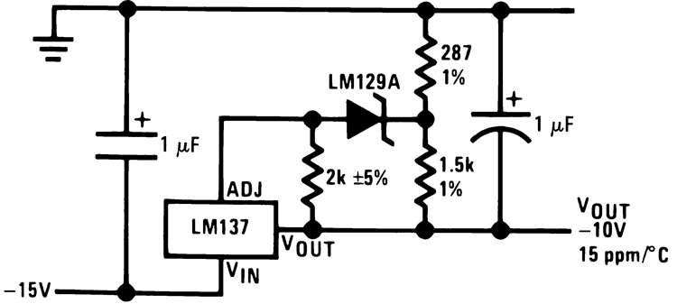
Using a high stability shunt voltage reference in the feedback path, such as the LM329, provides damping necessary for a stable, low noise output.
