SNVS778E May 1999 – January 2016 LM137 , LM337-N
PRODUCTION DATA.
- 1 Features
- 2 Applications
- 3 Description
- 4 Revision History
- 5 Pin Configuration and Functions
- 6 Specifications
- 7 Detailed Description
- 8 Application and Implementation
- 9 Power Supply Recommendations
- 10Layout
- 11Device and Documentation Support
- 12Mechanical, Packaging, and Orderable Information
Package Options
Mechanical Data (Package|Pins)
- NDT|3
Thermal pad, mechanical data (Package|Pins)
Orderable Information
7 Detailed Description
7.1 Overview
In operation, the LM137 and LM337-N develops a nominal −1.25-V reference voltage between the output and adjustment terminal. The reference voltage is impressed across program resistor R1 (120 Ω for example) and, because the voltage is constant, a constant current then flows through the output set resistor R2, giving an output voltage calculated by Equation 1.

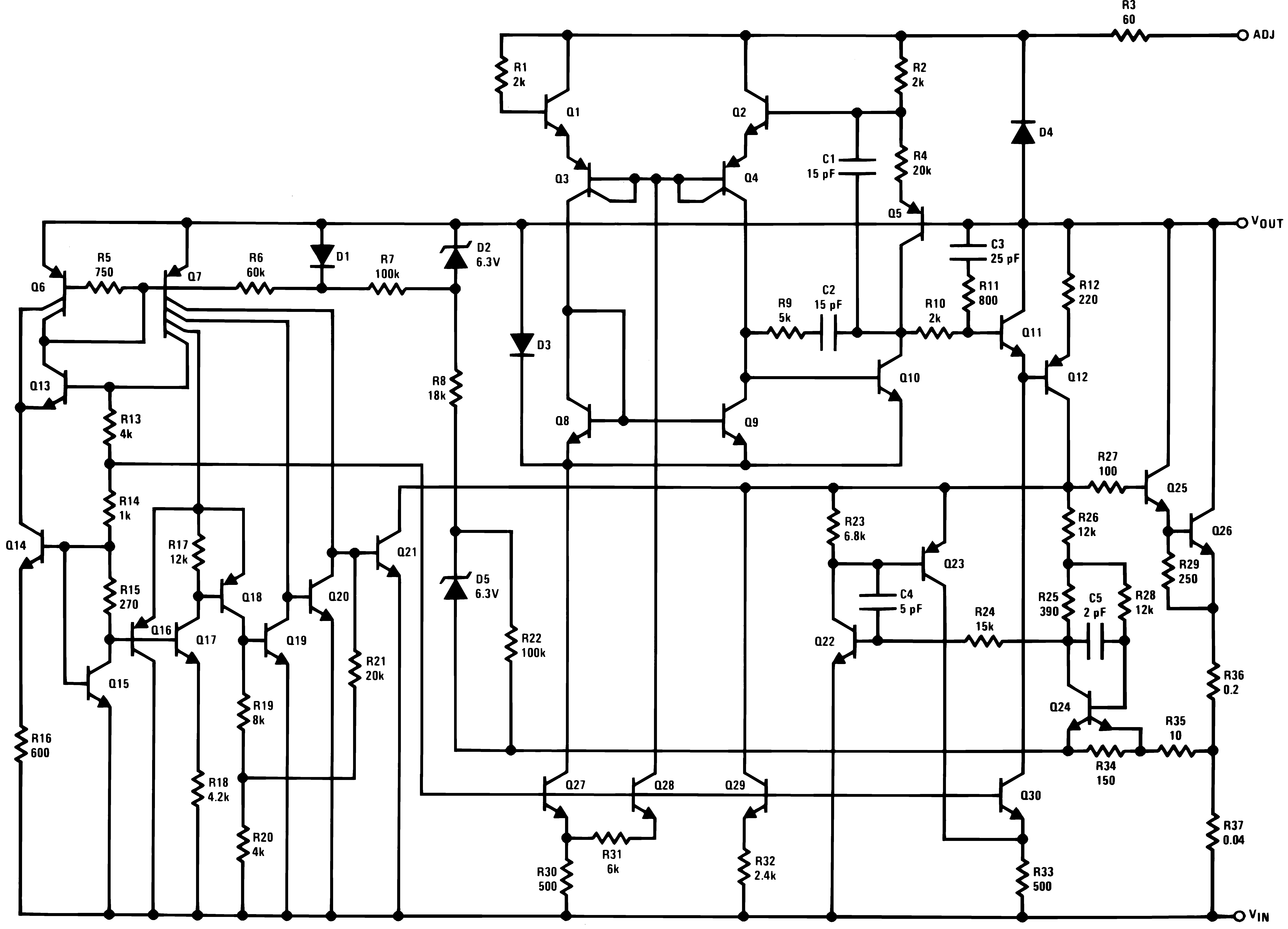
7.2 Functional Block Diagram

7.3 Feature Description
7.3.1 Thermal Regulation
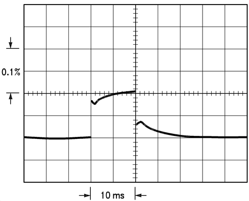
When power is dissipated in an IC, a temperature gradient occurs across the IC chip affecting the individual IC circuit components. With an IC regulator, this gradient can be especially severe because power dissipation is large. Thermal regulation is the effect of these temperature gradients on output voltage (in percentage output change) per Watt of power change in a specified time. Thermal regulation error is independent of electrical regulation or temperature coefficient, and occurs within 5 ms to 50 ms after a change in power dissipation. Thermal regulation depends on IC layout as well as electrical design. The thermal regulation of a voltage regulator is defined as the percentage change of VOUT, per Watt, within the first 10 ms after a step of power is applied. The LM137 device's specification is 0.02%/W, maximum.

VOUT = −10 V
VIN − VOUT = −40 V
IIL = 0 A → 0.25 A → 0 A
Vertical sensitivity, 5 mV/div
In Figure 13, a typical LM137 device's output drifts only 3 mV (or 0.03% of VOUT = −10 V) when a 10-W pulse is applied for 10 ms. This performance is thus well inside the specification limit of 0.02%/W × 10 W = 0.2% maximum. When the 10-W pulse is ended, the thermal regulation again shows a 3-mV step at the LM137 chip cools off.
NOTE
The load regulation error of about 8 mV (0.08%) is additional to the thermal regulation error.
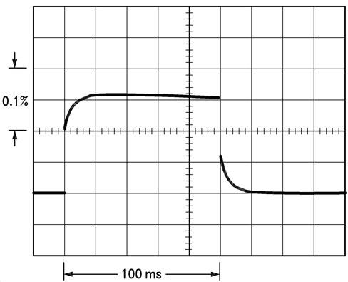
In Figure 14, when the 10-W pulse is applied for 100 ms, the output drifts only slightly beyond the drift in the first 10 ms, and the thermal error stays well within 0.1% (10 mV).

VOUT = −10 V
VIN − VOUT = −40 V
IL = 0 A → 0.25 A → 0 A
Horizontal sensitivity, 20 ms/div
7.4 Device Functional Modes
7.4.1 Protection Diodes
When external capacitors are used with any IC regulator, it is sometimes necessary to add protection diodes to prevent the capacitors from discharging through low current points into the regulator. Most 10-μF capacitors have low enough internal series resistance to deliver 20-A spikes when shorted. Although the surge is short, there is enough energy to damage parts of the IC.
When an output capacitor is connected to a negative output regulator and the input is shorted, the output capacitor pulls current out of the output of the regulator. The current depends on the value of the capacitor, the output voltage of the regulator, and the rate at which VIN is shorted to ground.
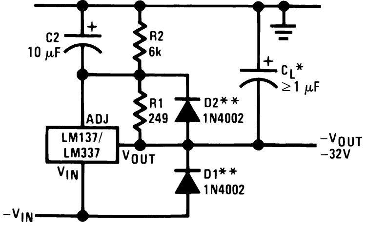
The bypass capacitor on the adjustment terminal can discharge through a low current junction. Discharge occurs when either the input, or the output, is shorted. Figure 15 shows the placement of the protection diodes.

**When C2 is larger than 10 μF and −VOUT is larger than −25V, D2 protects the LM137 in case the output is shorted