SNVS671F February   2011  – May 2019 LM21212-1

PRODUCTION DATA.  

  1. Features
  2. Applications
  3. Description
    1.     Device Images
      1.      Simplified Application Circuit
  4. Revision History
  5. Description
  6. Pin Configuration and Functions
    1.     Pin Functions
  7. Specifications
    1. 7.1 Absolute Maximum Ratings
    2. 7.2 ESD Ratings
    3. 7.3 Recommended Operating Conditions
    4. 7.4 Thermal Information
    5. 7.5 Electrical Characteristics
    6. 7.6 Typical Performance Characteristics
  8. Detailed Description
    1. 8.1 Overview
    2. 8.2 Functional Block Diagram
    3. 8.3 Feature Description
      1. 8.3.1 Frequency Synchronization
      2. 8.3.2 Precision Enable
      3. 8.3.3 UVLO
      4. 8.3.4 Current Limit
      5. 8.3.5 Short-Circuit Protection
      6. 8.3.6 Thermal Protection
      7. 8.3.7 Power-Good Flag
      8. 8.3.8 Light Load Operation
  9. Application and Implementation
    1. 9.1 Application Information
    2. 9.2 Typical Application
      1. 9.2.1 Detailed Design Procedure
        1. 9.2.1.1 Custom Design With WEBENCH® Tools
        2. 9.2.1.2 Output Voltage
        3. 9.2.1.3 Precision Enable
        4. 9.2.1.4 Soft Start
        5. 9.2.1.5 Inductor Selection
        6. 9.2.1.6 Output Capacitor Selection
        7. 9.2.1.7 Input Capacitor Selection
        8. 9.2.1.8 Control Loop Compensation
      2. 9.2.2 Application Curves
  10. 10Layout
    1. 10.1 Pcb Layout Considerations
    2. 10.2 Thermal Considerations
  11. 11Device and Documentation Support
    1. 11.1 Device Support
      1. 11.1.1 Third-Party Products Disclaimer
      2. 11.1.2 Development Support
        1. 11.1.2.1 Custom Design With Webench® Tools
    2. 11.2 Receiving Notification Of Documentation Updates
    3. 11.3 Community Resources
    4. 11.4 Trademarks
    5. 11.5 Electrostatic Discharge Caution
    6. 11.6 Glossary
  12. 12Mechanical, Packaging, And Orderable Information

Package Options

Mechanical Data (Package|Pins)
Thermal pad, mechanical data (Package|Pins)
Orderable Information

Inductor Selection

The inductor (L) used in the application will influence the ripple current and the efficiency of the system. The first selection criteria is to define a ripple current, ΔIL. In a buck converter, it is typically selected to run between 20% to 30% of the maximum output current. Figure 30 shows the ripple current in a standard buck converter operating in continuous conduction mode. Larger ripple current will result in a smaller inductance value, which will lead to a lower series resistance in the inductor, and improved efficiency. However, larger ripple current will also cause the device to operate in discontinuous conduction mode at a higher average output current.
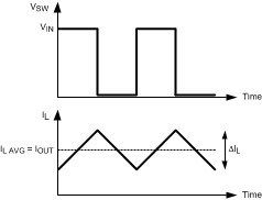
LM21212-1 30119907.gifFigure 30. Switch And Inductor Current Waveforms

Once the ripple current has been determined, the appropriate inductor size can be calculated using the following equation:

Equation 5. LM21212-1 30119906.gif