SNOSBJ3E November 1999 – December 2014 LM139-N , LM239-N , LM2901-N , LM339-N
PRODUCTION DATA.
- 1 Features
- 2 Applications
- 3 Description
- 4 Revision History
- 5 Pin Configuration and Functions
- 6 Specifications
- 7 Detailed Description
- 8 Application and Implementation
- 9 Power Supply Recommendations
- 10Layout
- 11Device and Documentation Support
- 12Mechanical, Packaging, and Orderable Information
Package Options
Mechanical Data (Package|Pins)
- J|14
Thermal pad, mechanical data (Package|Pins)
Orderable Information
7 Detailed Description
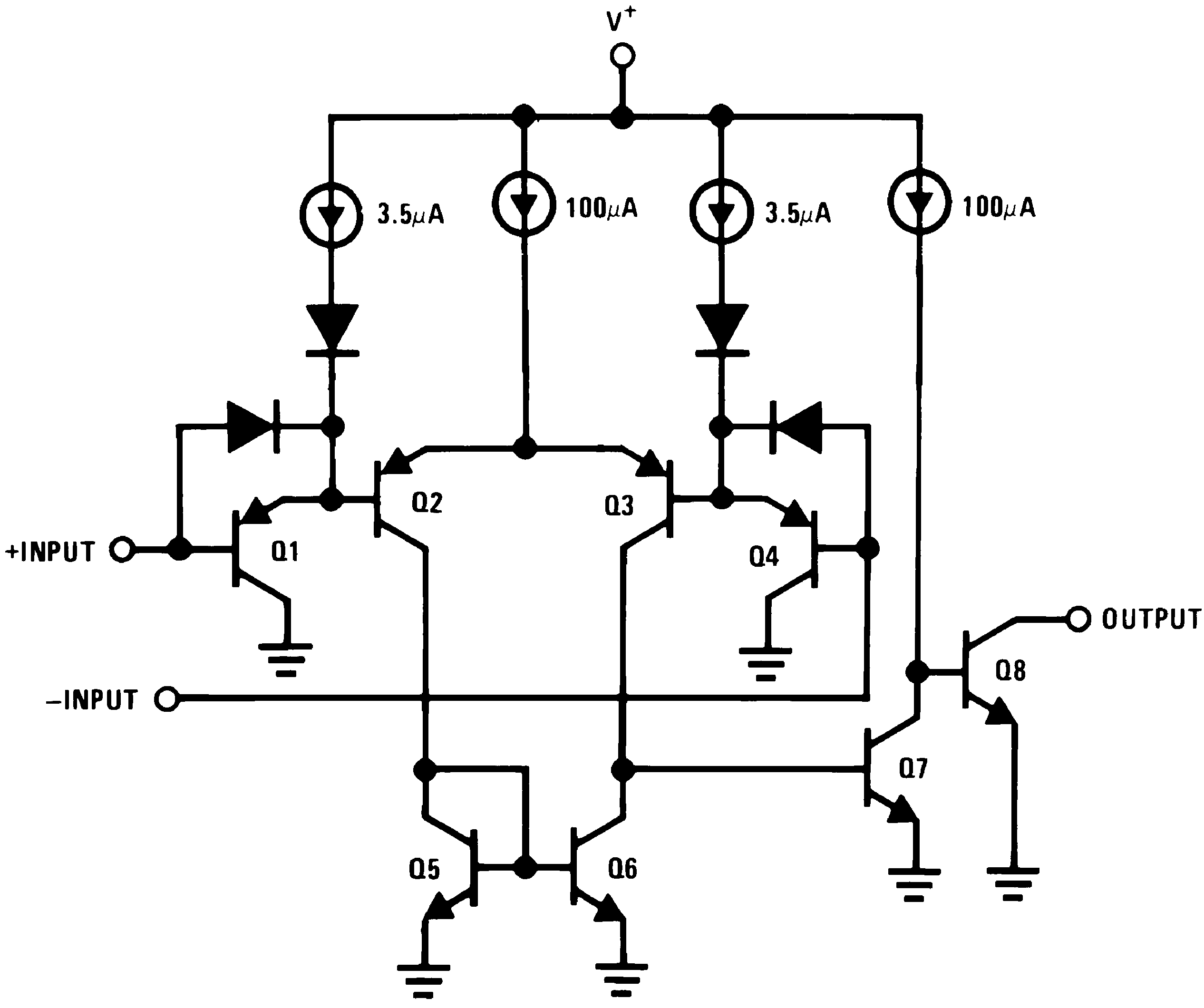
7.1 Overview
The LM139/LM239/LM339 family of devices is a monolithic quad of independently functioning comparators designed to meet the needs for a medium-speed, TTL compatible comparator for industrial applications. Since no antisaturation clamps are used on the output such as a Baker clamp or other active circuitry, the output leakage current in the OFF state is typically 0.1 nA. This makes the device ideal for system applications where it is desired to switch a node to ground while leaving it totally unaffected in the OFF state. Other features include single supply, low voltage operation with an input common mode range from ground up to approximately one volt below VCC . The output is an uncommitted collector so it may be used with a pullup resistor and a separate output supply to give switching levels from any voltage up to 36V down to a V CE SAT above ground (approximately 100 mV), sinking currents up to 16 mA. The open collector output configuration allows the device to be used in wired-OR configurations, such as a window comparators.
In addition it may be used as a single pole switch to ground, leaving the switched node unaffected while in the OFF state. Power dissipation with all four comparators in the OFF state is typically 4 mW from a single 5-V supply (1 mW/comparator).
7.3 Feature Description
The LMx39-N series are high-gain, wide bandwidth devices which, like most comparators, can easily oscillate if the output lead is inadvertently allowed to capacitively couple to the inputs through stray capacitance. This shows up only during the output voltage transition intervals as the comparator changes states. Reducing the input resistors to < 10 kΩ reduces the feedback signal levels and finally, adding even a small amount (1 to 10 mV) of positive feedback (hysteresis) causes such a rapid transition that oscillations due to stray feedback are not possible. Simply socketing the IC and attaching resistors to the pins will cause input-output oscillations during the small transition intervals unless hysteresis is used. If the input signal is a pulse waveform, with relatively fast rise and fall times, hysteresis is not required.
The differential input voltage may be larger than V+ without damaging the device. Protection should be provided to prevent the input voltages from going negative more than −0.3 VDC (at 25°C). An input clamp diode can be used as shown in the applications section.
The output of the LMx39-N series is the uncommitted collector of a grounded-emitter NPN output transistor. Many collectors can be tied together to provide an output OR'ing function. An output pullup resistor can be connected to any available power supply voltage within the permitted supply voltage range and there is no restriction on this voltage due to the magnitude of the voltage which is applied to the V+ terminal of the LM139A package. The output can also be used as a simple SPST switch to ground (when a pullup resistor is not used). The amount of current which the output device can sink is limited by the drive available (which is independent of V+) and the β of this device. When the maximum current limit is reached (approximately 16 mA), the output transistor will come out of saturation and the output voltage will rise very rapidly. The output saturation voltage is limited by the approximately 60-Ω RSAT of the output transistor. The low offset voltage of the output transistor (4 mV) allows the output to clamp essentially to ground level for small load currents.
7.4 Device Functional Modes
A basic comparator circuit is used for converting analog signals to a digital output. The output is HIGH when the voltage on the non-inverting (+IN) input is greater than the inverting (-IN) input. The output is LOW when the voltage on the noninverting (+IN) input is less than the inverting (-IN) input. The inverting input (-IN) is also commonly referred to as the "reference" or "VREF" input.
All pins of any unused comparators should be tied to the negative supply.
The bias network of the LMx39-N series establishes a drain current which is independent of the magnitude of the power supply voltage over the range of from 2 VDC to 30 VDC.