SNOSBJ3E November 1999 – December 2014 LM139-N , LM239-N , LM2901-N , LM339-N
PRODUCTION DATA.
- 1 Features
- 2 Applications
- 3 Description
- 4 Revision History
- 5 Pin Configuration and Functions
- 6 Specifications
- 7 Detailed Description
- 8 Application and Implementation
- 9 Power Supply Recommendations
- 10Layout
- 11Device and Documentation Support
- 12Mechanical, Packaging, and Orderable Information
Package Options
Mechanical Data (Package|Pins)
- J|14
Thermal pad, mechanical data (Package|Pins)
Orderable Information
10 Layout
10.1 Layout Guidelines
Try to minimize parasitic impedances on the inputs to avoid oscillation. Any positive feedback used as hysteresis should place the feedback components as close as possible to the input pins. Take care to ensure that the output pins do not couple to the inputs. This can occur through capacitive coupling if the traces are too close and lead to oscillations on the output.
The optimum bypass capacitor placement is closest to the V+ and ground pins. Take care to minimize the loop area formed by the bypass capacitor connection between V+ and ground. The ground pin should be connected to the PCB ground plane at the pin of the device. The feedback components should be placed as close to the device as possible minimizing strays.
10.2 Layout Example
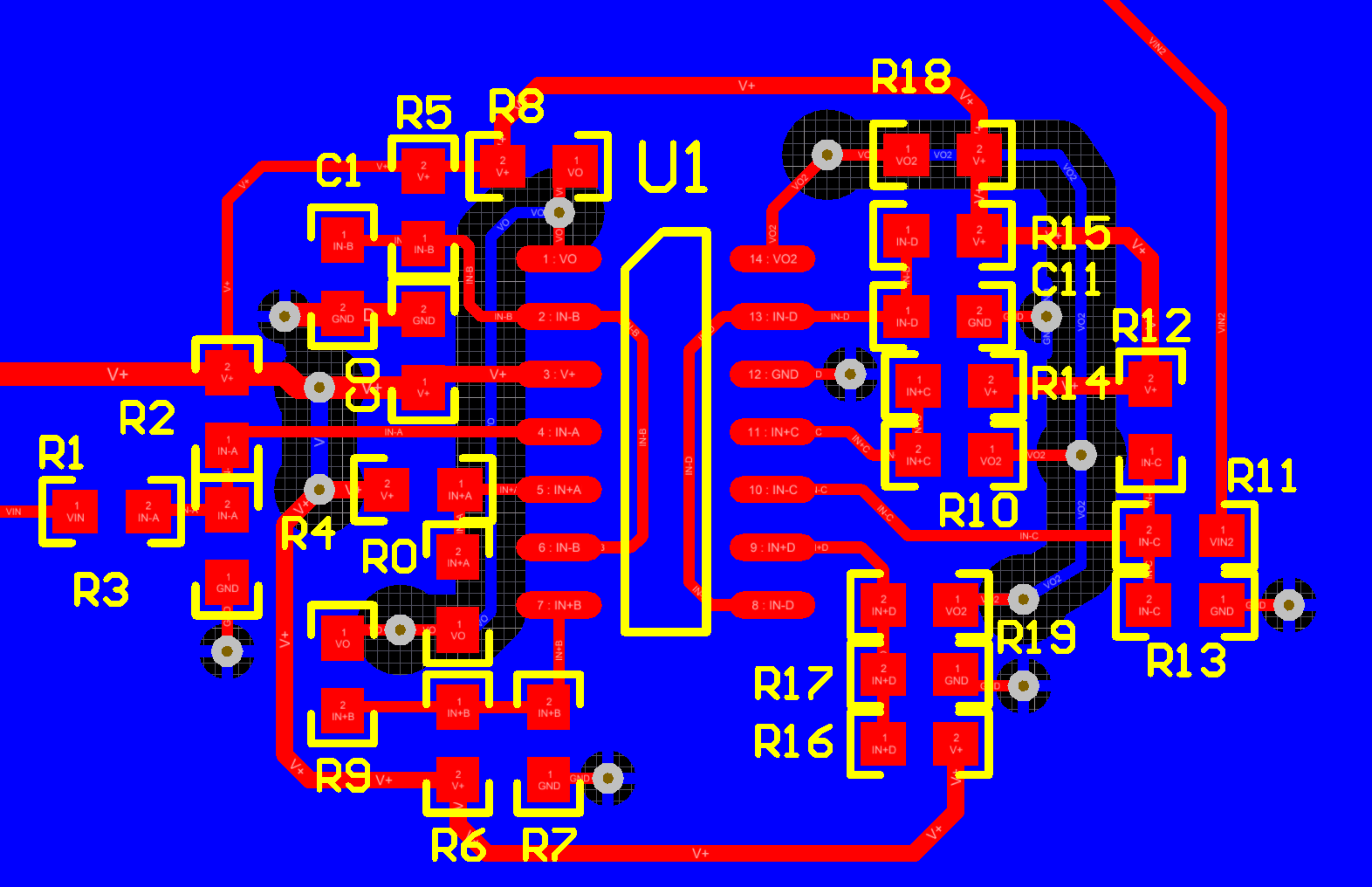 Figure 38. Layout Example