SNOSBJ3E November 1999 – December 2014 LM139-N , LM239-N , LM2901-N , LM339-N
PRODUCTION DATA.
- 1 Features
- 2 Applications
- 3 Description
- 4 Revision History
- 5 Pin Configuration and Functions
- 6 Specifications
- 7 Detailed Description
- 8 Application and Implementation
- 9 Power Supply Recommendations
- 10Layout
- 11Device and Documentation Support
- 12Mechanical, Packaging, and Orderable Information
Package Options
Mechanical Data (Package|Pins)
- J|14
Thermal pad, mechanical data (Package|Pins)
Orderable Information
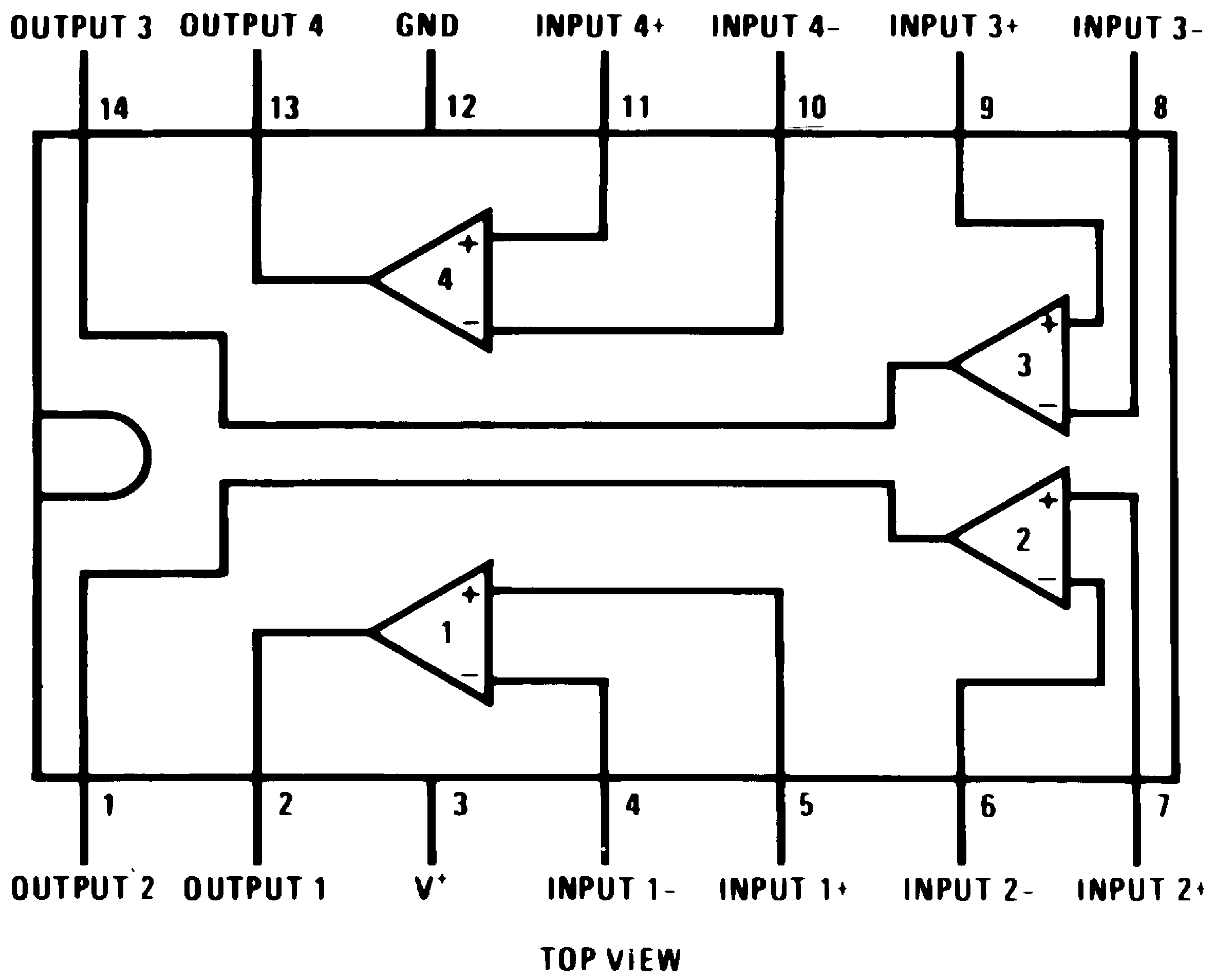
5 Pin Configuration and Functions
J, D and NFF Package
14-Pin CDIP, SOIC, PDIP
Top View
14-Pin CLGA Package
Top View
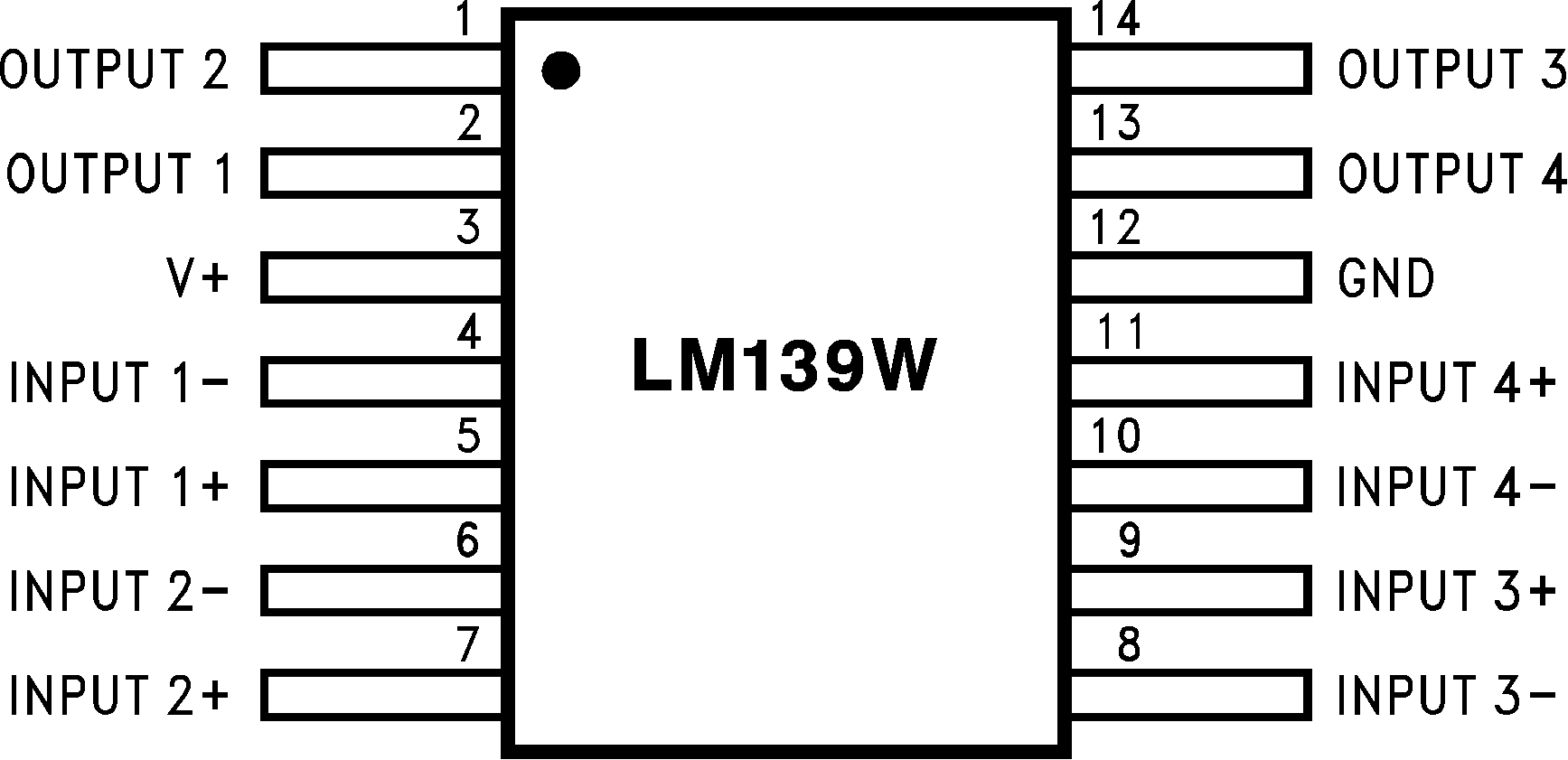
Pin Functions
| PIN | I/O | DESCRIPTION | |
|---|---|---|---|
| NO. | NAME | ||
| 1 | OUTPUT2 | O | Output, Channel 2 |
| 2 | OUTPUT1 | O | Output, Channel 1 |
| 3 | V+ | P | Positive Supply |
| 4 | INPUT1- | I | Inverting Input, Channel 1 |
| 5 | INPUT1+ | I | Noninverting Input, Channel 1 |
| 6 | INPUT2- | I | Inverting Input, Channel 2 |
| 7 | INPUT2+ | I | Noninverting Input, Channel 2 |
| 8 | INPUT3- | I | Inverting Input, Channel 3 |
| 9 | INPUT3+ | I | Noninverting Input, Channel 3 |
| 10 | INPUT4- | I | Inverting Input, Channel 4 |
| 11 | INPUT4+ | I | Noninverting Input, Channel 4 |
| 12 | GND | P | Ground |
| 13 | OUTPUT4 | O | Output, Channel 4 |
| 14 | OUTPUT3 | O | Output, Channel 3 |