SNVS593J October 2008 – November 2014 LM25085 , LM25085-Q1
PRODUCTION DATA.
- 1 Features
- 2 Applications
- 3 Description
- 4 Revision History
- 5 Pin Configuration and Functions
- 6 Specifications
- 7 Detailed Description
- 8 Application and Implementation
- 9 Power Supply Recommendations
- 10Layout
- 11Device and Documentation Support
- 12Mechanical, Packaging, and Orderable Information
Package Options
Mechanical Data (Package|Pins)
Thermal pad, mechanical data (Package|Pins)
- DGN|8
Orderable Information
8 Application and Implementation
NOTE
Information in the following applications sections is not part of the TI component specification, and TI does not warrant its accuracy or completeness. TI’s customers are responsible for determining suitability of components for their purposes. Customers should validate and test their design implementation to confirm system functionality.
8.1 Application Information
The LM25085/LM25085-Q1 devices are step-down DC-DC converters. The devices are typically used to convert a higher DC voltage to a lower DC voltage. Use the following design procedure to select component values. Alternately, use the WEBENCH® software to generate a complete design. The WEBENCH software uses an iterative design procedure and accesses a comprehensive database of components when generating a design. This section presents a simplified discussion of the design process.
8.2 Typical Application
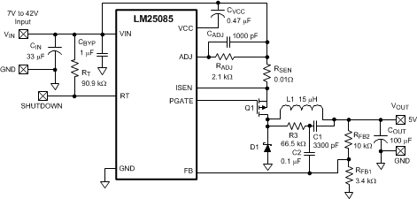 Figure 24. LM25085 Typical Application
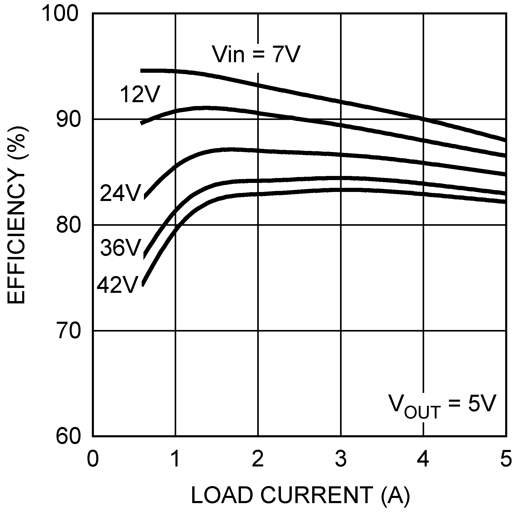
8.2.1 Design Requirements
The procedure for calculating the external components is illustrated with the following design example. Referring to Figure 24, the circuit is to be configured for the following specifications:
- VOUT = 5V
- VIN = 7V to 42V, 12V Nominal
- Maximum load current (IOUT(max)) = 5A
- Minimum load current (IOUT(min)) = 600mA (for continuous conduction mode)
- Switching Frequency (FSW) = 300kHz
- Maximum allowable output ripple (VOS) = 5mVp-p
- Selected PFET: Vishay Si7465
8.2.2 Detailed Design Procedure
8.2.2.1 RFB1 and RFB2
These resistors set the output voltage. The ratio of these resistors is calculated from:
For this example, RFB2 / RFB1 = 3. Typically, RFB1 and RFB2 should be chosen from standard value resistors in the range of 1kΩ to 20kΩ which satisfy the above ratio. For this example, RFB2 = 10kΩ, and RFB1 = 3.4kΩ.
8.2.2.2 RT, PFET
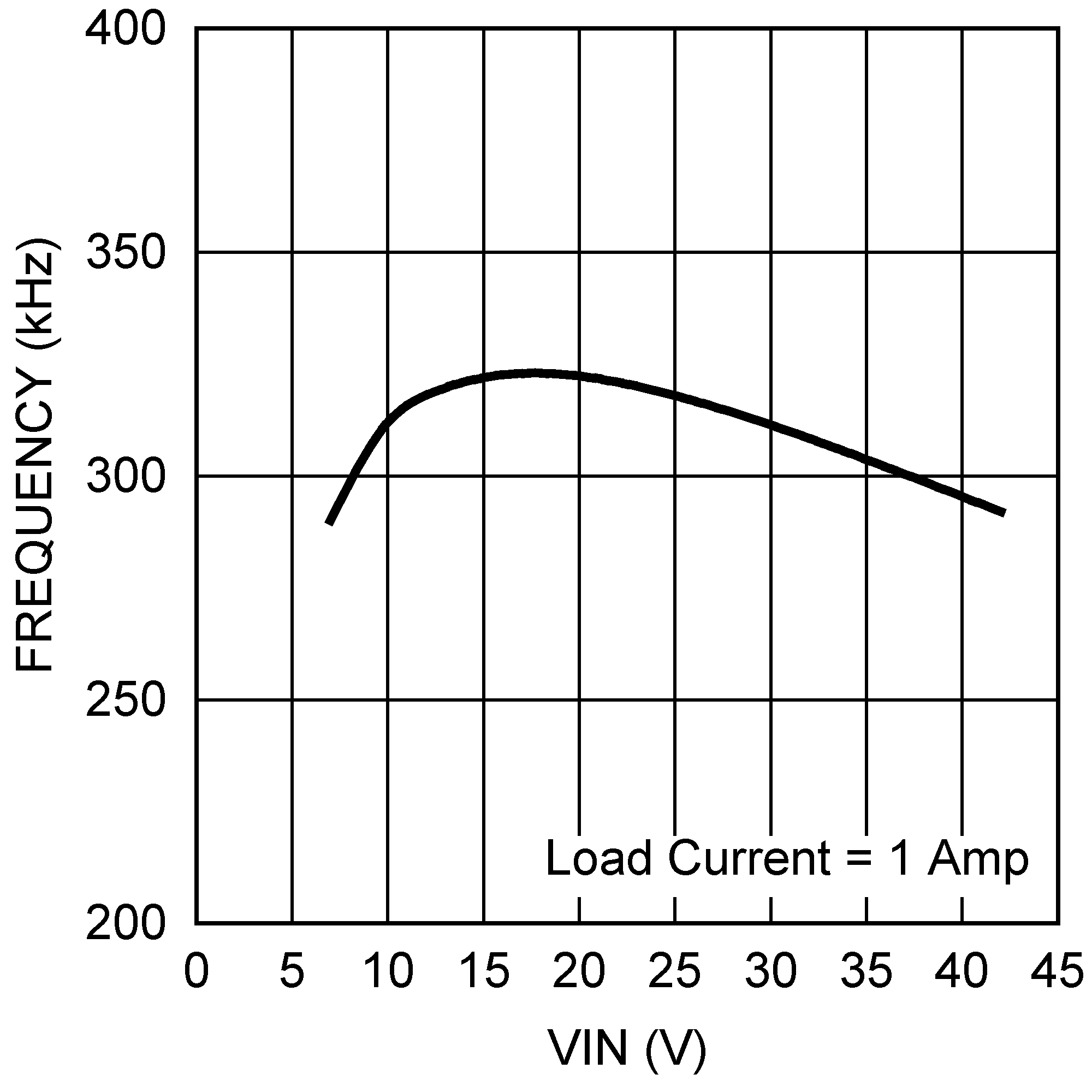
Before selecting the RT resistor, the PFET must be selected as its turn-on and turn-off delays affect the calculated value of RT. For the Vishay Si7465 PFET, the difference of its typical turn-off and turn-on delays is 57ns. Using Equation 5 at nominal input voltage, RT calculates to be:

A standard value 90.9kΩ resistor is selected. Using Equation 3 the minimum on-time at the PGATE pin, which occurs at maximum input voltage (42V), is calculated to be 381ns. This minimum one-shot period is sufficiently longer than the minimum recommended value of 150ns. The minimum on-time at the SW node (junction of Q1, D1, L1) is longer due to the delay added by the PFET (57ns). Therefore the minimum SW node on-time is 438ns at 42V. The maximum on-time at the SW node is calculated to be 2.55µs at 7V.
8.2.2.3 L1
The main parameter controlled by the inductor value is the current ripple amplitude (IOR). See Figure 25. The minimum load current for continuous conduction mode is used to determine the maximum allowable ripple such that the inductor current valley does not fall to zero. Continuous conduction mode operation at minimum load current is not a requirement of the LM25085, but serves as a guideline for selecting L1. For this example, the maximum ripple current is:
If the minimum load current of the application is zero, a good initial estimate for the maximum ripple current (IOR(max)) is 20% of the maximum load current. The ripple calculated in Equation 17 is then used in the following equation to calculate L1:
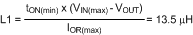
A standard value 15µH inductor is selected. Using this inductance value, the maximum ripple current amplitude, which occurs at maximum input voltage, is calculated to be 1.08 Ap-p. The peak current (IPK) at maximum load current is 5.54A. However, the current rating of the selected inductor must be based on the maximum current limit value calculated below.
 Figure 25. Inductor Current Waveform
8.2.2.4 RSEN, RADJ
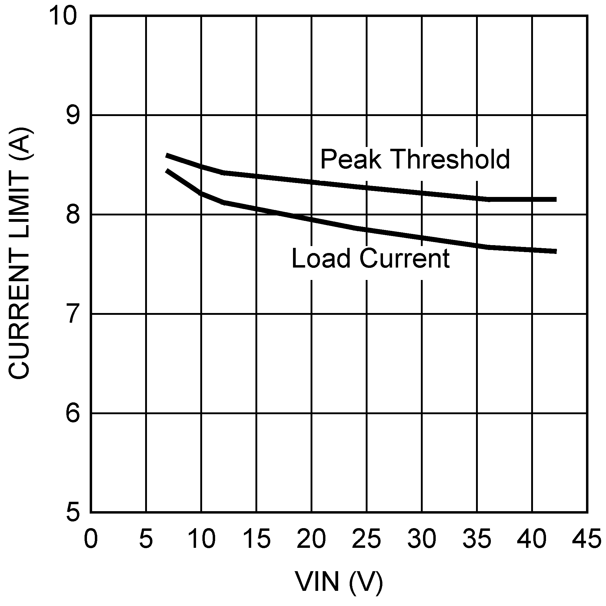
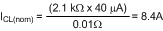
To achieve good current limit accuracy and avoid over designing the power stage components, the sense resistor method is used for current limiting in this example. A standard value 10mΩ resistor is selected for RSEN, resulting in a 50mV drop at maximum load current, and a maximum 0.25W power dissipation in the resistor. Since the LM25085 uses peak current detection, the minimum value for the current limit threshold must be equal to the maximum load current (5A) plus half the maximum ripple amplitude calculated above:
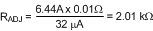
At this current level the voltage across RSEN is 55.4mV. Adding the current limit comparator offset of 9mV (max) increases the required current limit threshold to 6.44A. Using Equation 9 with the minimum value for the ADJ pin current (32µA), the required RADJ resistor is calculated to be:
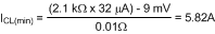
A standard value 2.1kΩ resistor is selected. The nominal current limit threshold is:
Using the tolerances for the ADJ pin current and the current limit comparator offset, the maximum current limit threshold is calculated to be:
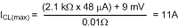
The minimum current limit threshold is:
The load current in each case is equal to the current limit threshold minus half the current ripple amplitude. The recommended value of 1000pF for CADJ is used in this example.
8.2.2.5 COUT
Since the maximum allowed output ripple voltage is very low in this example (5mVp-p), the minimum ripple configuration (R3, C1, and C2 in the Functional Block Diagram) must be used. The resulting ripple at VOUT is then due to the inductor’s ripple current passing through COUT. This capacitor’s value can be selected based on the maximum allowable ripple voltage at VOUT, or based on transient response requirements. The following calculation, based on ripple voltage, provides a first order result for the value of COUT:
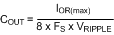
where IOR(max) is the maximum ripple current calculated above, and VRIPPLE is the allowable ripple at VOUT.
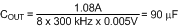
A 100µF capacitor is selected. Typically the ripple amplitude will be higher than the calculations indicate due to the capacitor’s ESR.
8.2.2.6 R3, C1, C2
The minimum ripple configuration uses these three components to generate the ripple voltage required at the FB pin since there is insufficient ripple at VOUT. A minimum of 25mVp-p must be applied to the FB pin to obtain stable constant frequency operation. R3 and C1 are selected to generate a sawtooth waveform at their junction, and that waveform is AC coupled to the FB pin via C2. The values of the three components are determined using the following procedure:
First calculate VA = VOUT - (VSW x (1 – (VOUT/VIN(min))))
where VSW is the absolute value of the voltage at the SW node during the off-time, typically 0.5V to 1V depending on the diode D1. Using a typical value of 0.65V, VA calculates to 4.81V. VA is the nominal DC voltage at the R3/C1 junction, and is used in the next equation to calculate the R-C product:
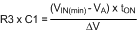
where tON is the maximum on-time (at minimum input voltage), and ΔV is the desired ripple amplitude at the R3/C1 junction. For ripple voltage of 25 mVp-p:
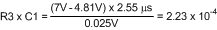
R3 and C1 are then selected from standard value components to produce the product calculated above. Typical values for C1 are 3000pF to 10,000pF, and R3 is typically from 10kΩ to 300kΩ. C2 is then chosen large compared to C1, typically 0.1µF. For this example, 3300pF is chosen for C1, requiring R3 to be 67.7kΩ. A standard value 66.5kΩ resistor is selected.
8.2.2.7 Alternate Output Ripple Configurations
The minimum ripple configuration with C1, C2 and R3 in the example circuit, Figure 24, results in a low ripple amplitude at VOUT determined mainly by the characteristics of the output capacitor and the ripple current in L1. This configuration allows multiple ceramic capacitors to be used for VOUT if the output voltage is provided to several places on the PC board. However, if a slightly higher level of ripple at VOUT is acceptable in the application, and distributed capacitance is not used, the ripple required for the FB comparator pin can be generated with fewer external components using the circuits shown in Figure 26 and Figure 27.
8.2.2.7.1 Reduced Ripple Configuration
In Figure 26, R3, C1 and C2 are removed (compared to Layout Example). A low value resistor (R4) is added in series with COUT, and a capacitor (Cff) is added across RFB2. Ripple is generated at VOUT by the inductor’s ripple current flowing through R4, and that ripple voltage is passed to the FB pin via Cff. The ripple at VOUT can be set as low as 25mVp-p since it is not attenuated by RFB2 and RFB1. The minimum value for R4 is calculated from:

where IOR(min) is the minimum ripple current, which occurs at minimum input voltage. The minimum value for Cff is determined from:

where tON(max) is the maximum on-time, which occurs at minimum VIN. The next larger standard value capacitor should be used for Cff.
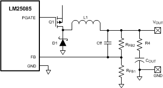 Figure 26. Reduced Ripple Configuration
8.2.2.7.2 Lowest Cost Configuration
This configuration, shown in Figure 27, is the same as Figure 26 except Cff is removed. Since the ripple voltage at VOUT is attenuated by RFB2 and RFB1, the minimum ripple required at VOUT is equal to:
VRIP(min) = 25mV x (RFB2 + RFB1)/RFB1
The minimum value for R4 is calculated from:

where IOR(min) is the minimum ripple current, which occurs at minimum input voltage.
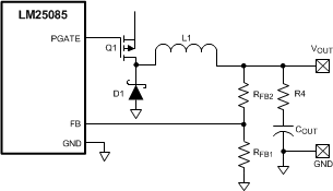 Figure 27. Lowest Cost Ripple Generating Configuration
8.2.2.8 CIN, CBYP
These capacitors limit the voltage ripple at VIN by supplying most of the switch current during the on-time. At maximum load current, when Q1 is switched on, the current through Q1 suddenly increases to the lower peak of the inductor’s ripple current, then ramps up to the upper peak, and then drops to zero at turn-off. The average current during the on-time is the load current. For a worst case calculation, these capacitors must supply this average load current during the maximum on-time, while limiting the voltage drop at VIN. For this example, 0.5V is selected as the maximum allowable droop at VIN.
The minimum input capacitance is calculated from:
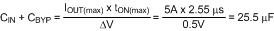
A 33µF electrolytic capacitor is selected for CIN, and a 1µF ceramic capacitor is selected for CBYP. Due to the ESR of CIN, the ripple at VIN will likely be higher than the calculation indicates, and therefore it may be desirable to increase CIN to 47µF or 68µF. CBYP must be located as close as possible to the VIN and GND pins of the LM25085. The voltage rating for both capacitors must be at least 42V. The RMS ripple current rating for the input capacitors must also be considered. A good approximation for the required ripple current rating is IRMS > IOUT/2.
8.2.2.9 D1
A Schottky diode is recommended. Ultra-fast recovery diodes are not recommended as the high speed transitions at the SW node may affect the regulator’s operation due to diode reverse recovery transients. The diode must be rated for the maximum input voltage, and the worst case current limit level. The average power dissipation in the diode is calculated from:
where VF is the diode forward voltage drop, and D is the on-time duty cycle. Using Equation 1, the minimum duty cycle occurs at maximum input voltage, and is calculated to be ≊11.9% in this example. The diode power dissipation calculates to be:
8.2.2.10 CVCC
The capacitor at the VCC pin (from VIN to VCC) provides not only noise filtering and stability for the VCC regulator, but also provides the surge current for the PFET gate drive. The typical recommended value for CVCC is 0.47µF. A good quality, low ESR, ceramic capacitor is recommended. CVCC must be located as close as possible to the VIN and VCC pins. If the selected PFET has a Total Gate Charge specification of 100nC or larger, or if the circuit is required to operate at input voltages below 7V, a larger capacitor may be required. The maximum recommended value for CVCC is 1µF.
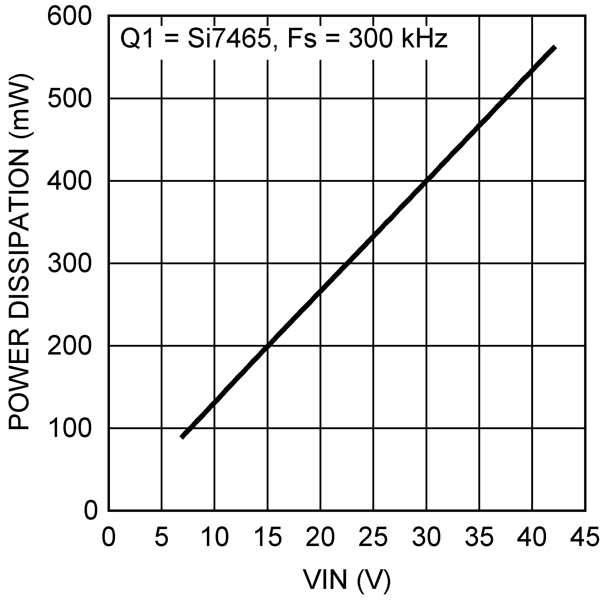
8.2.2.11 IC Power Dissipation
The maximum power dissipated in the LM25085 package is calculated using Equation 14 at the maximum input voltage. The Total Gate Charge for the Si7465 PFET is specified to be 40nC (max) in the data sheet. Therefore the total power dissipation within the LM25085 is calculated to be:
Using an HVSSOP-PowerPAD-8 package with a θJA of 46°C/W produces a temperature rise of 26°C from junction to ambient.