SNVS593J October 2008 – November 2014 LM25085 , LM25085-Q1
PRODUCTION DATA.
- 1 Features
- 2 Applications
- 3 Description
- 4 Revision History
- 5 Pin Configuration and Functions
- 6 Specifications
- 7 Detailed Description
- 8 Application and Implementation
- 9 Power Supply Recommendations
- 10Layout
- 11Device and Documentation Support
- 12Mechanical, Packaging, and Orderable Information
Package Options
Mechanical Data (Package|Pins)
Thermal pad, mechanical data (Package|Pins)
- DGN|8
Orderable Information
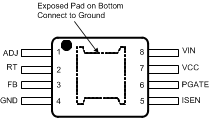
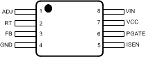
5 Pin Configuration and Functions
HVSSOP-PowerPad™
8-Lead DGN0008A
Top View
VSSOP
8-Lead DGK0008A
Top View
WSON
8-Lead NGQ0008A
Top View
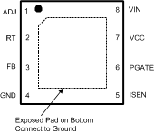
Pin Functions
| PIN | I/O | DESCRIPTION | |
|---|---|---|---|
| NAME | NO. | ||
| ADJ | 1 | I | Current Limit Adjust - The current limit threshold is set by an external resistor from VIN to ADJ in conjunction with the external sense resistor or the PFET’s RDS(ON). |
| RT | 2 | I | On-time control and shutdown - An external resistor from VIN to RT sets the buck switch on-time and switching frequency. Grounding this pin shuts down the controller. |
| FB | 3 | I | Voltage Feedback from the regulated output - Input to the regulation and over-voltage comparators. The regulation level is 1.25V. |
| GND | 4 | - | Circuit Ground - Ground reference for all internal circuitry. |
| ISEN | 5 | I | Current sense input for current limit detection. Connect to the PFET drain when using RDS(ON) current sense. Connect to the PFET source and the sense resistor when using a current sense resistor. |
| PGATE | 6 | O | Gate Driver Output - Connect to the gate of the external PFET. |
| VCC | 7 | O | Output of the gate driver bias regulator - Output of the negative voltage regulator (relative to VIN) that biases the PFET gate driver. A low ESR capacitor is required from VIN to VCC, located as close as possible to the pins. |
| VIN | 8 | I | Input supply voltage - The operating input range is from 4.5V to 42V. A low ESR bypass capacitor must be located as close as possible to the VIN and GND pins. |
| EP | - | Exposed Pad - Exposed pad on the underside of the package (HVSSOP-PowerPAD-8 and WSON only). This pad is to be soldered to the PC board ground plane to aid in heat dissipation. | |