SNVS593J October 2008 – November 2014 LM25085 , LM25085-Q1
PRODUCTION DATA.
- 1 Features
- 2 Applications
- 3 Description
- 4 Revision History
- 5 Pin Configuration and Functions
- 6 Specifications
- 7 Detailed Description
- 8 Application and Implementation
- 9 Power Supply Recommendations
- 10Layout
- 11Device and Documentation Support
- 12Mechanical, Packaging, and Orderable Information
Package Options
Mechanical Data (Package|Pins)
Thermal pad, mechanical data (Package|Pins)
- DGN|8
Orderable Information
6 Specifications
6.1 Absolute Maximum Ratings
| See (1)(1) | MIN | MAX | UNIT |
|---|---|---|---|
| VIN to GND | -0.3 | 45 | V |
| ISEN to GND | -3 | VIN + 0.3 | V |
| ADJ to GND | -0.3 | VIN + 0.3 | V |
| RT, FB to GND | -0.3 | 7 | V |
| VIN to VCC, VIN to PGATE | -0.3 | 10 | V |
(1) If Military/Aerospace specified devices are required, please contact the Texas Instruments Sales Office/ Distributors for availability and specifications.
6.2 Handling Ratings - LM25085
| MIN | MAX | UNIT | |||
|---|---|---|---|---|---|
| Tstg | Storage temperature range | -65 | 150 | °C | |
| V(ESD) | Electrostatic discharge | Human body model (HBM), per ANSI/ESDA/JEDEC JS-001, all pins(1) | 2 | kV | |
| Charged device model (CDM), per JEDEC specification JESD22-C101, all pins(2) | 750 | V | |||
(1) JEDEC document JEP155 states that 500-V HBM allows safe manufacturing with a standard ESD control process.
(2) JEDEC document JEP157 states that 250-V CDM allows safe manufacturing with a standard ESD control process.
6.3 Handling Ratings - LM25085-Q1
| MIN | MAX | UNIT | ||||
|---|---|---|---|---|---|---|
| Tstg | Storage temperature range | -65 | 150 | °C | ||
| V(ESD) | Electrostatic discharge | Human body model (HBM), per AEC Q100-002(1) | 2 | kV | ||
| Charged device model (CDM), per AEC Q100-011 | Corner pins 1, 4, 5, 8 | 750 | V | |||
| Other pins | 750 | |||||
(1) AEC Q100-002 indicates HBM stressing is done in accordance with the ANSI/ESDA/JEDEC JS-001 specification.
6.4 Recommended Operating Conditions
Over operating free-air temperature range (unless otherwise noted)| MIN | MAX | UNIT | ||
|---|---|---|---|---|
| VIN Voltage | 4.5 | 42 | V | |
| Junction Temperature | −40 | 125 | °C | |
6.5 Thermal Information
| THERMAL METRIC(1) | LM25085 | LM25085 / Q-1 | LM25085 | UNIT | |
|---|---|---|---|---|---|
| VSSOP | HVSSOP-PowerPAD | WSON | |||
| 8 PINS | 8 PINS | 8 PINS | |||
| RθJA | Junction-to-ambient thermal resistance | 153 | 54.1 | 44.8 | °C/W |
| RθJC | Junction-to-case (top) thermal resistance | 52.5 | 49.1 | 39.4 | |
| RθJB | Junction-to-board thermal resistance | 71.9 | 26.7 | 11.6 | |
| ψJT | Junction-to-top characterization parameter | 4.6 | 1.3 | 0.3 | |
| ψJB | Junction-to-board characterization parameter | 70.8 | 26.5 | 11.6 | |
| RθJC(bot) | Junction-to-case (bottom) thermal resistance | 29 | 3.6 | 5.0 | |
(1) For more information about traditional and new thermal metrics, see the IC Package Thermal Metrics application report, SPRA953.
6.6 Electrical Characteristics
Typical values correspond to TJ = 25°C. Minimum and maximum limits apply over –40°C to 125°C junction temperature range, unless otherwise stated. VIN = 24V, RT = 100kΩ unless otherwise stated. (See (5)).| PARAMETER | TEST CONDITIONS | MIN | TYP | MAX | UNIT | |
|---|---|---|---|---|---|---|
| VIN PIN | ||||||
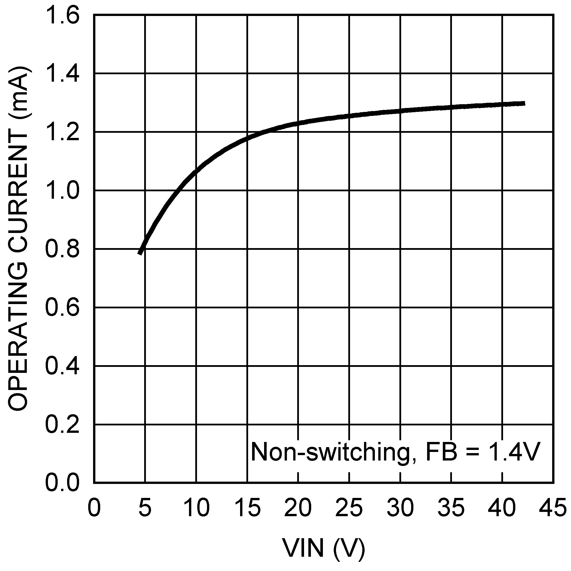
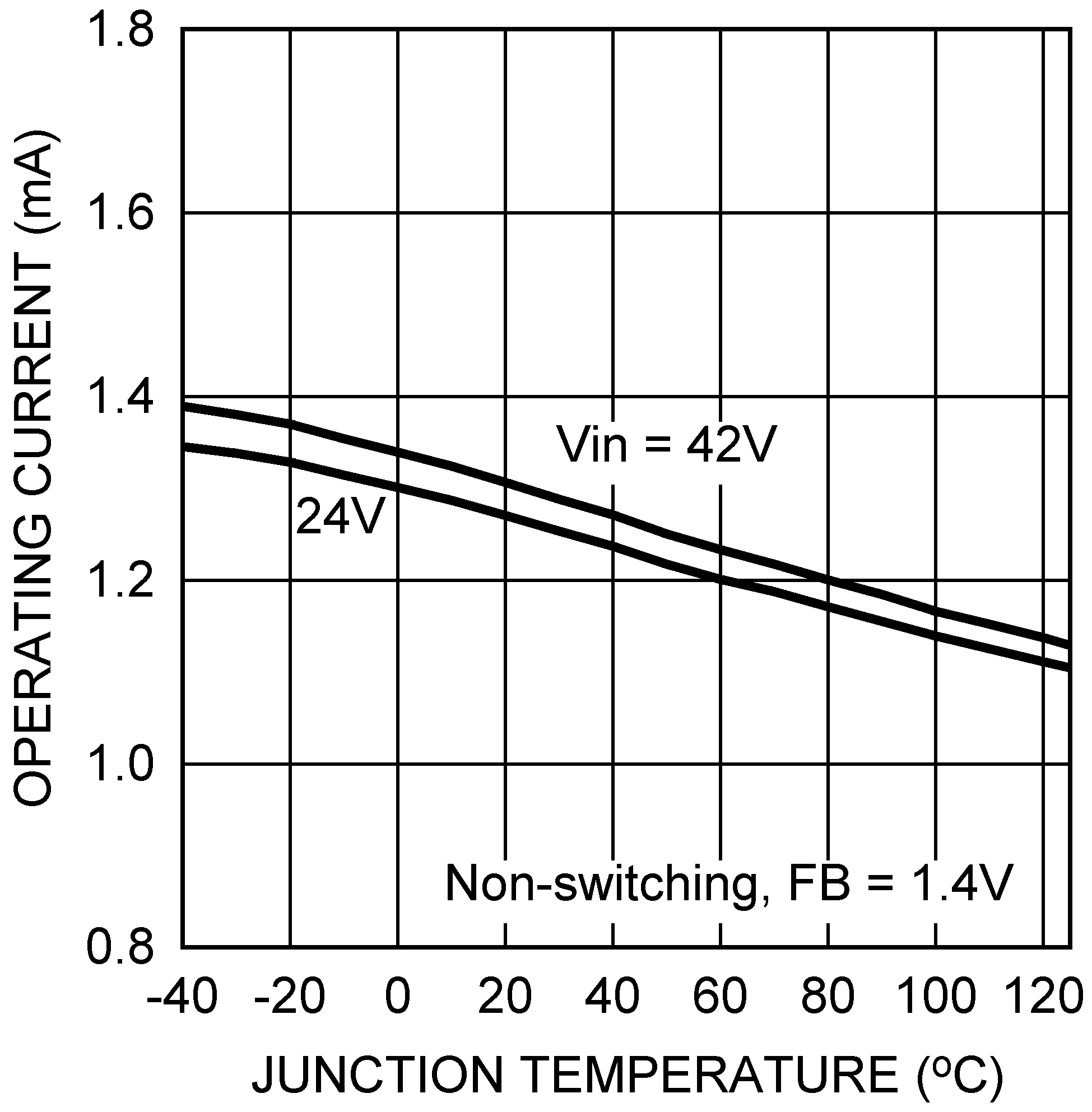
| IIN | Operating Current | Non-Switching, FB = 1.4V (3) | 1.25 | 1.75 | mA | |
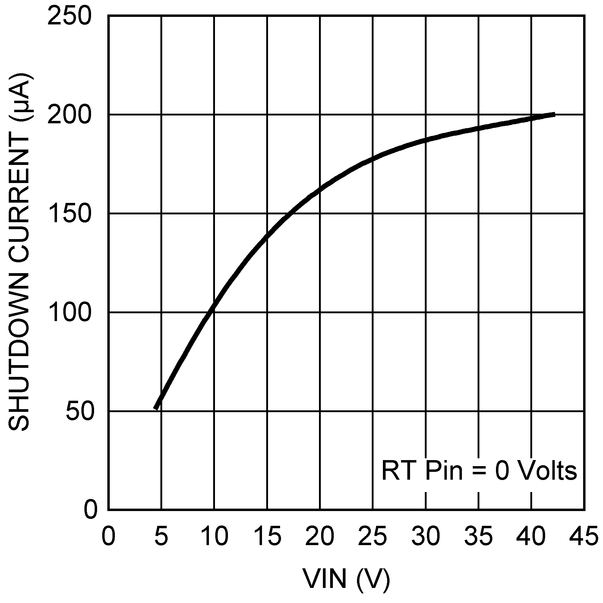
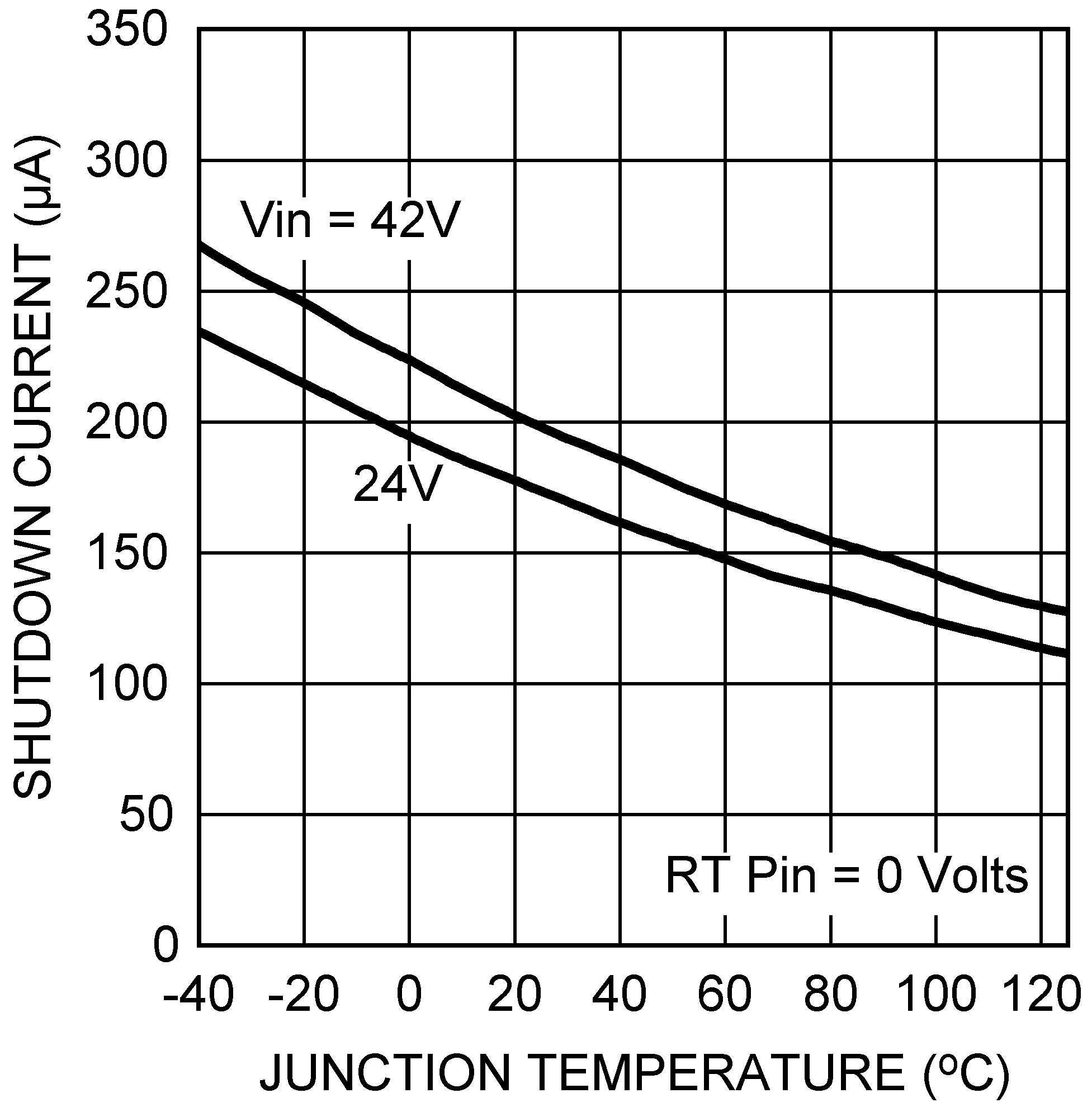
| IQ | Shutdown Current | RT = 0V (3) | 175 | 300 | µA | |
| VCC REGULATOR (2) | ||||||
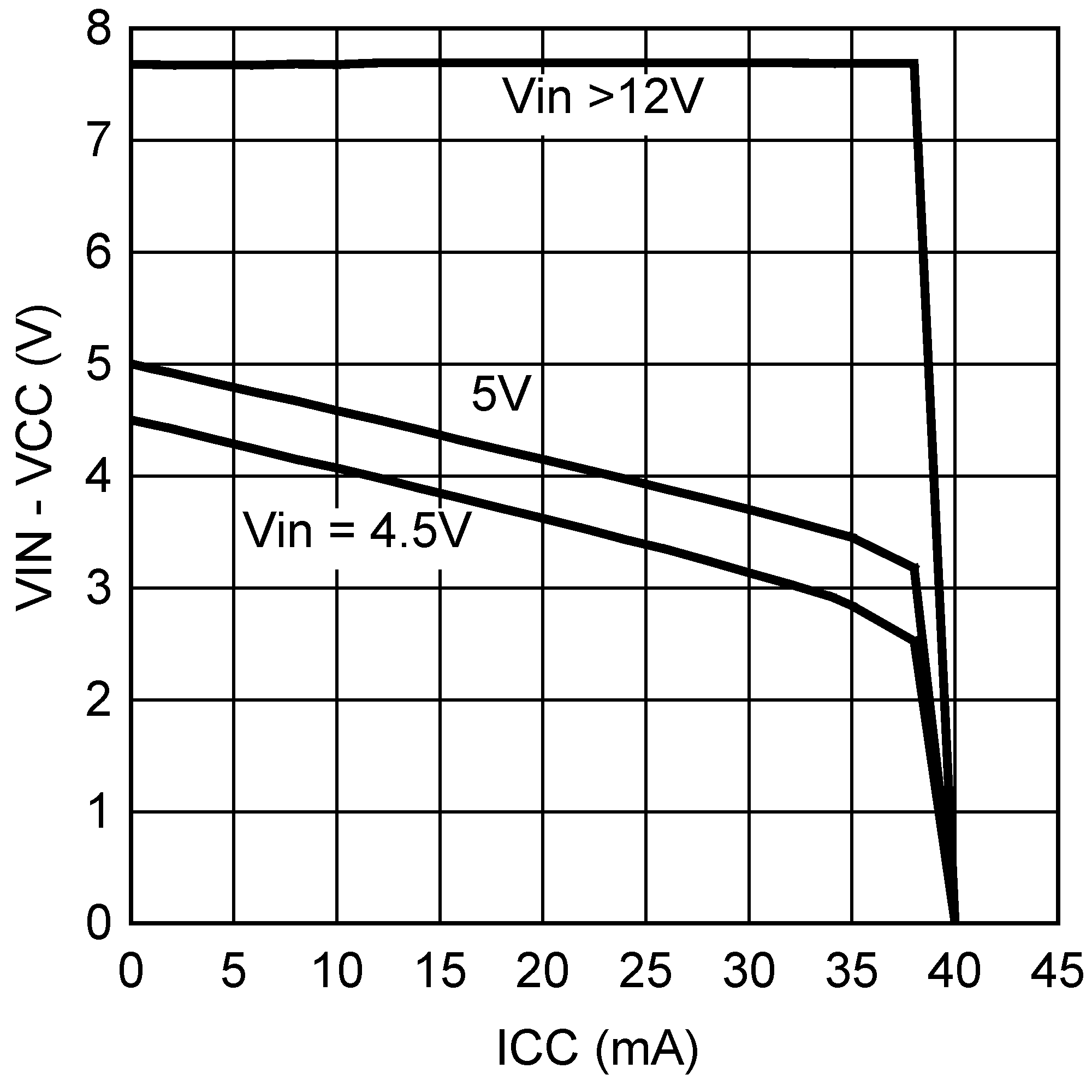
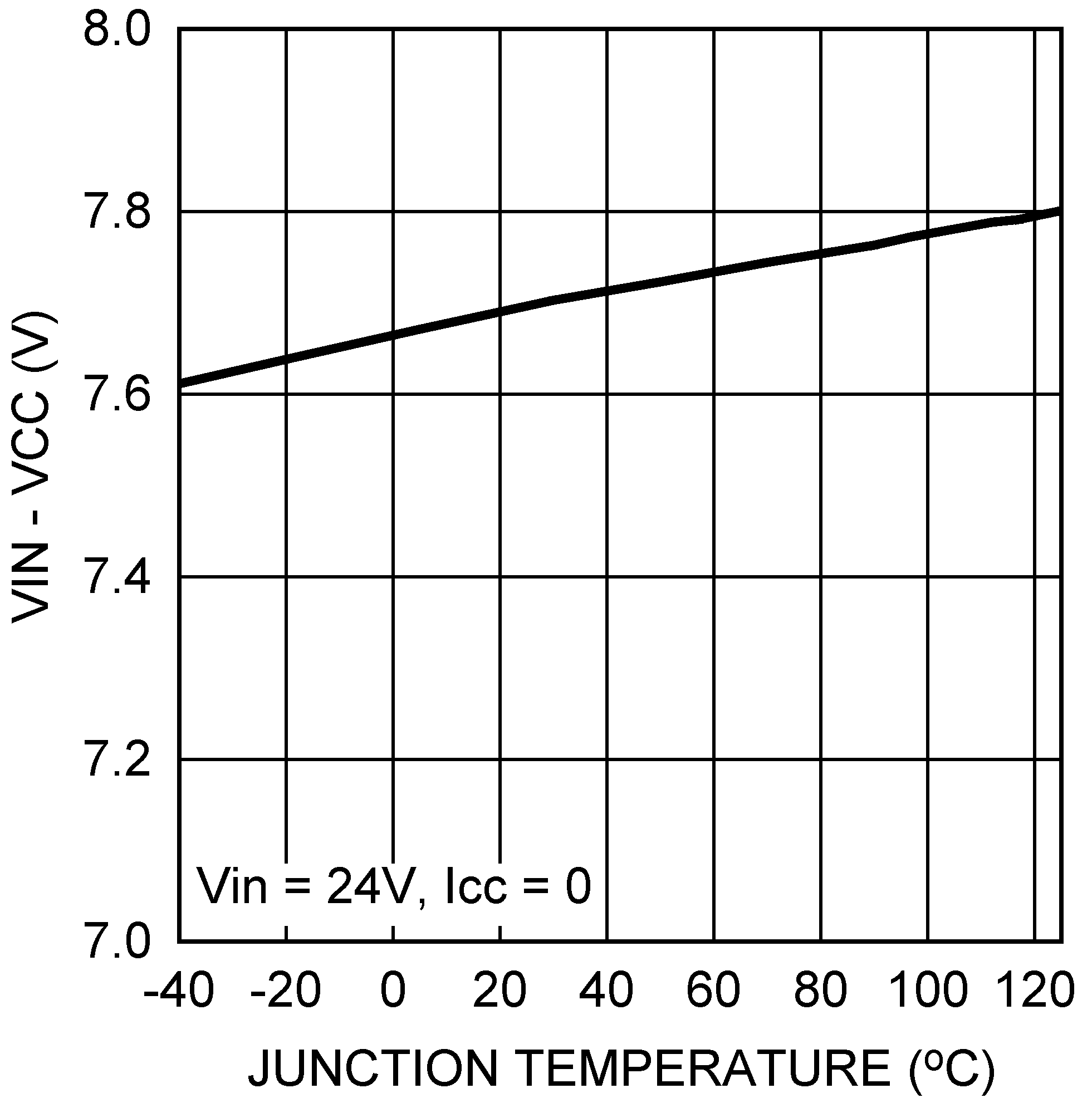
| VCC(reg) | VIN - VCC | Vin = 9V, FB = 1.4V, ICC = 0mA | 6.9 | 7.7 | 8.5 | V |
| Vin = 9V, FB = 1.4V, ICC = 20mA | 7.7 | V | ||||
| Vin = 42V, FB = 1.4V, ICC = 0mA | 7.7 | V | ||||
| UVLOVcc | VCC Under-Voltage Lock-Out Threshold | VCC Increasing | 3.8 | V | ||
| UVLOVcc Hysteresis | VCC Decreasing | 260 | mV | |||
| VCC(CL) | VCC Current Limit | FB = 1.4V | 20 | 40 | mA | |
| PGATE PIN | ||||||
| VPGATE(HI) | PGATE High Voltage | PGATE Pin = Open | VIN -0.1 | VIN | V | |
| VPGATE(LO) | PGATE Low Voltage | PGATE Pin = Open | VCC | VCC+0.1 | V | |
| VPGATE(HI)4.5 | PGATE High Voltage at Vin = 4.5V | PGATE Pin = Open | VIN -0.1 | VIN | V | |
| VPGATE(LO)4.5 | PGATE Low Voltage at Vin = 4.5V | PGATE Pin = Open | VCC | VCC+0.1 | V | |
| IPGATE | Driver Output Source Current | VIN = 12V, PGATE = VIN - 3.5V | 1.75 | A | ||
| Driver Output Sink Current | VIN = 12V, PGATE = VIN - 3.5V | 1.5 | A | |||
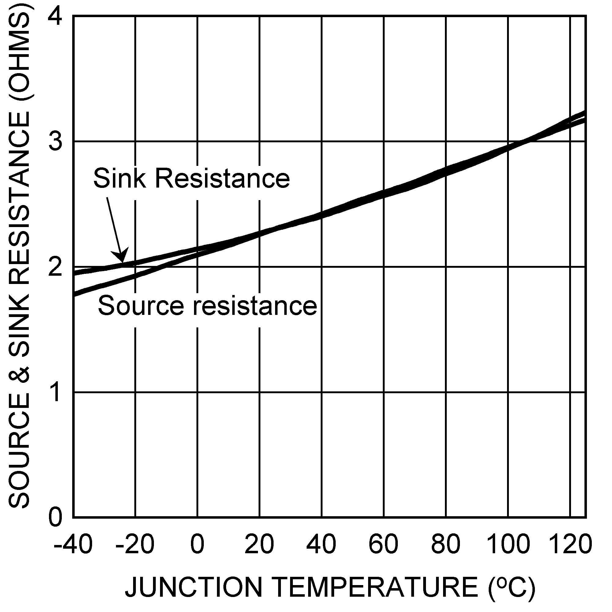
| RPGATE | Driver Output Resistance | Source current = 500mA | 2.3 | Ω | ||
| Sink current = 500mA | 2.3 | Ω | ||||
| CURRENT LIMIT DETECTION | ||||||
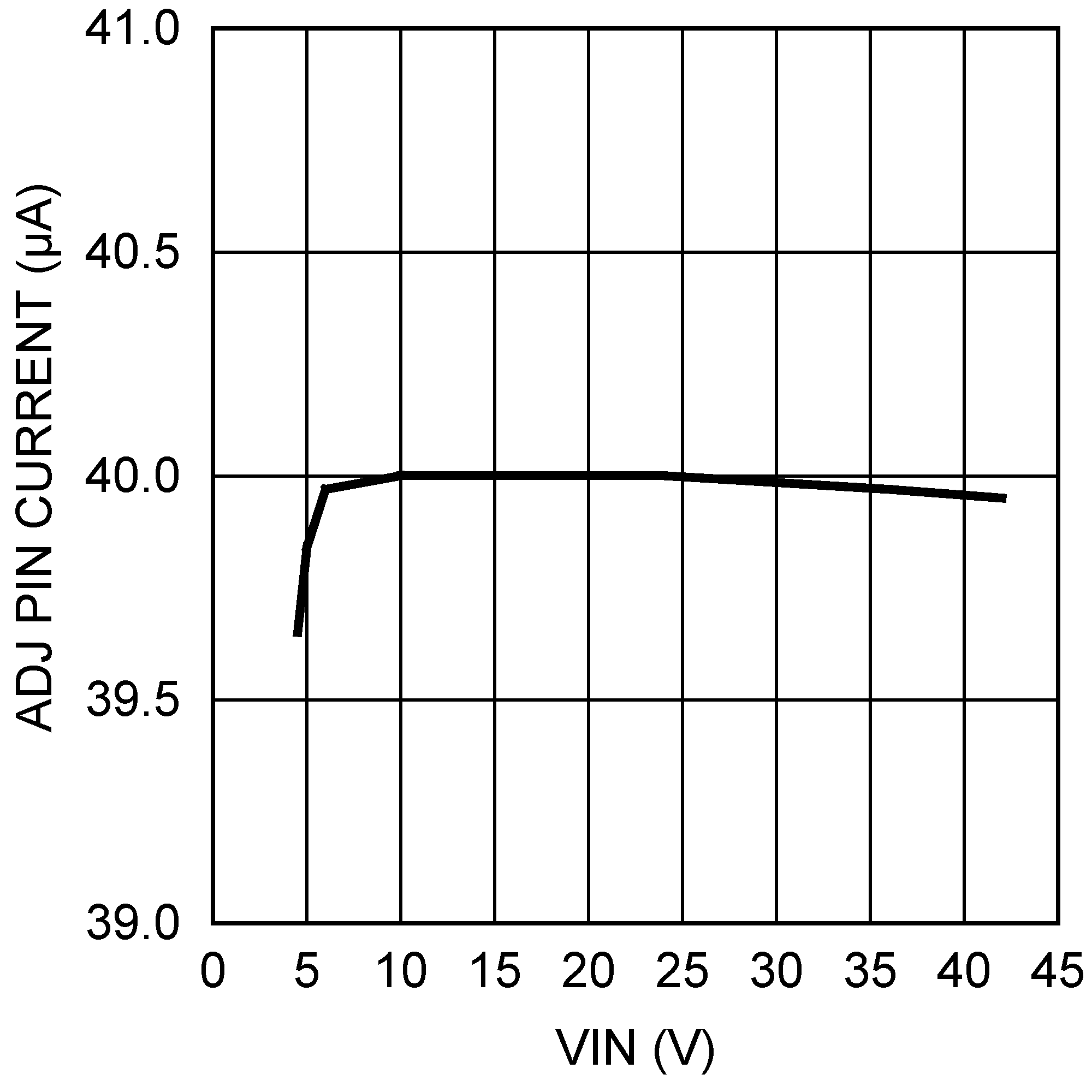
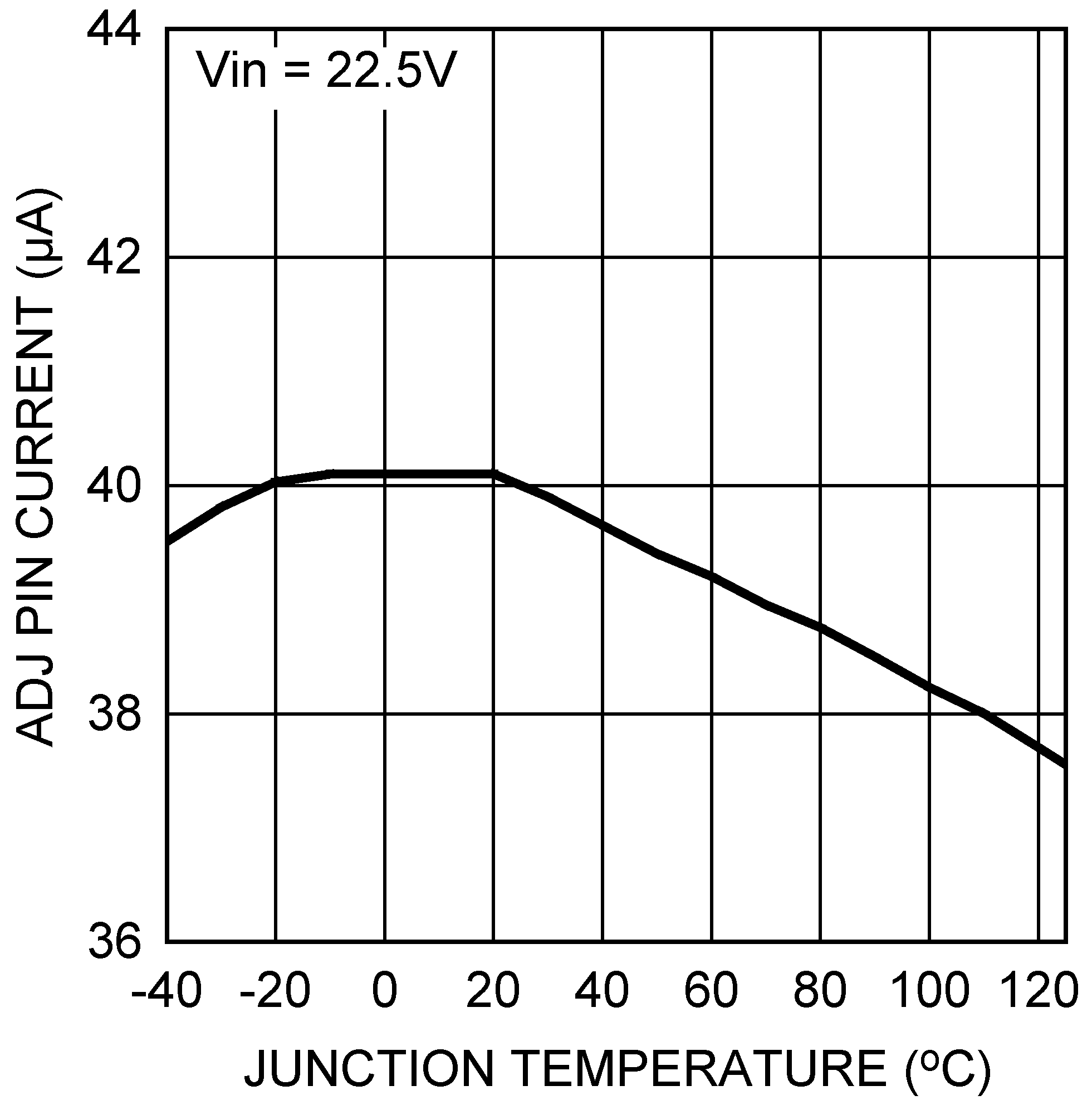
| IADJ | ADJUST Pin Current Source | VADJ = 22.5V | 32 | 40 | 48 | µA |
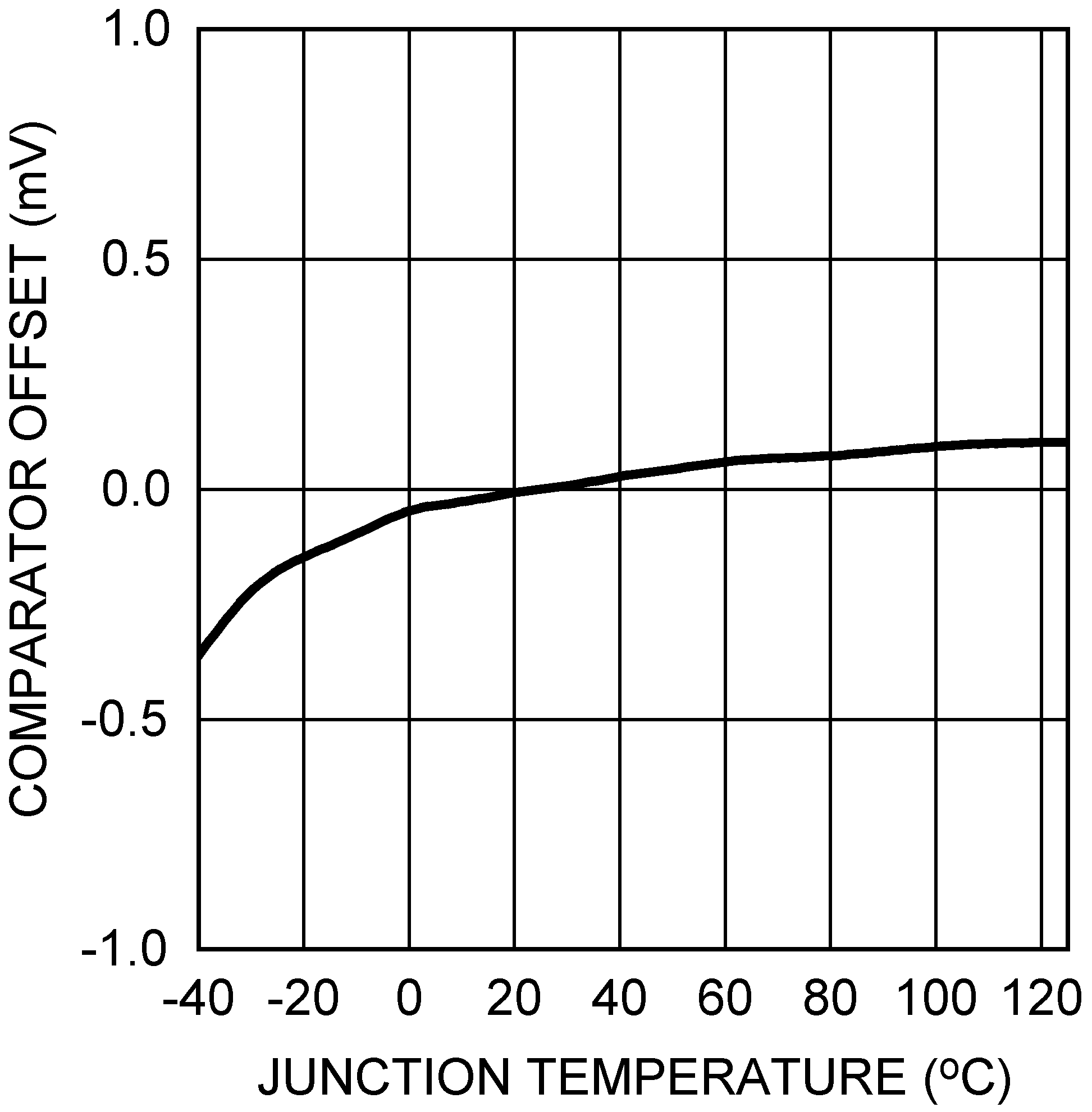
| VCL OFFSET | Current Limit Comparator Offset | VADJ = 22.5V, VADJ - VISEN | -9 | 0 | 9 | mV |
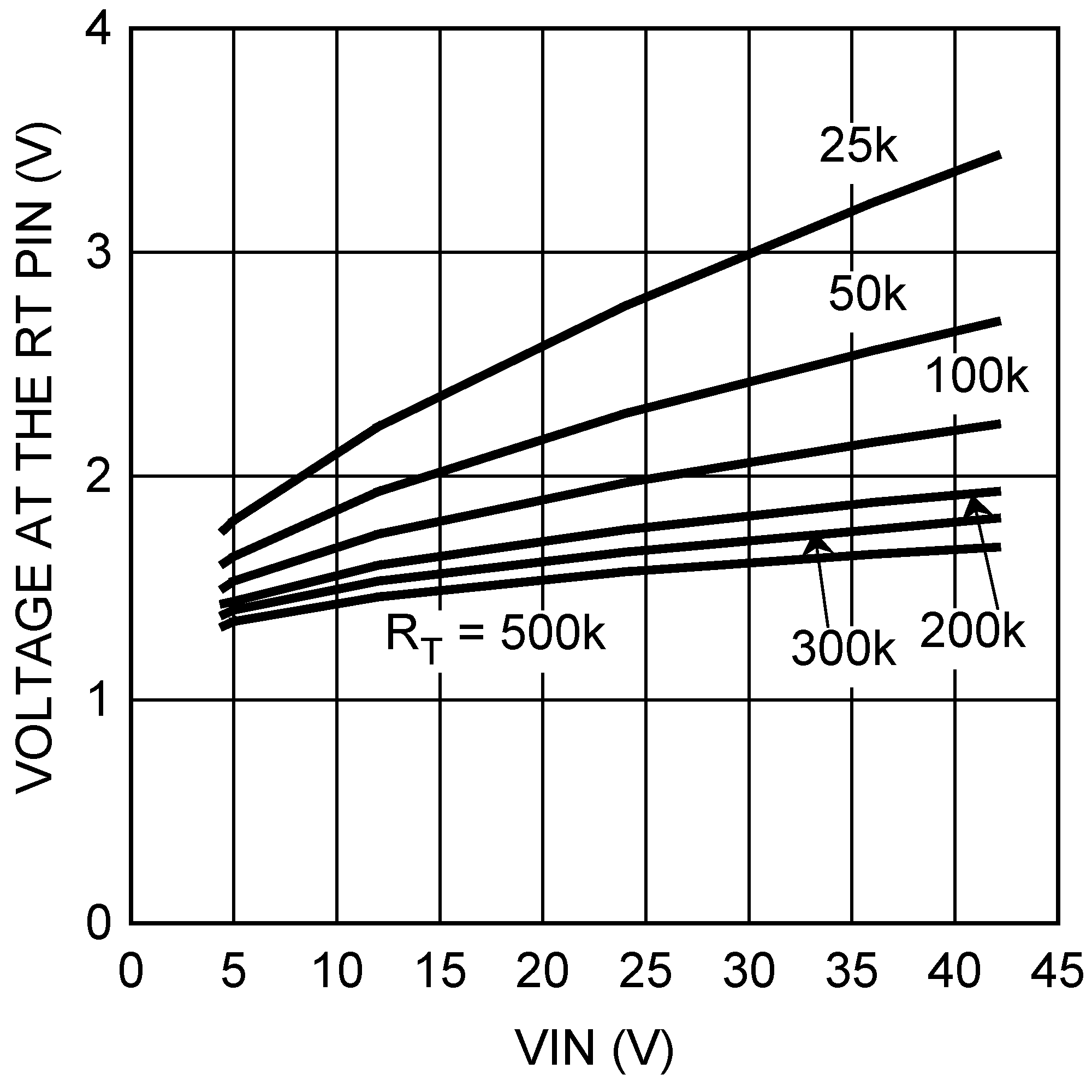
| RT PIN | ||||||
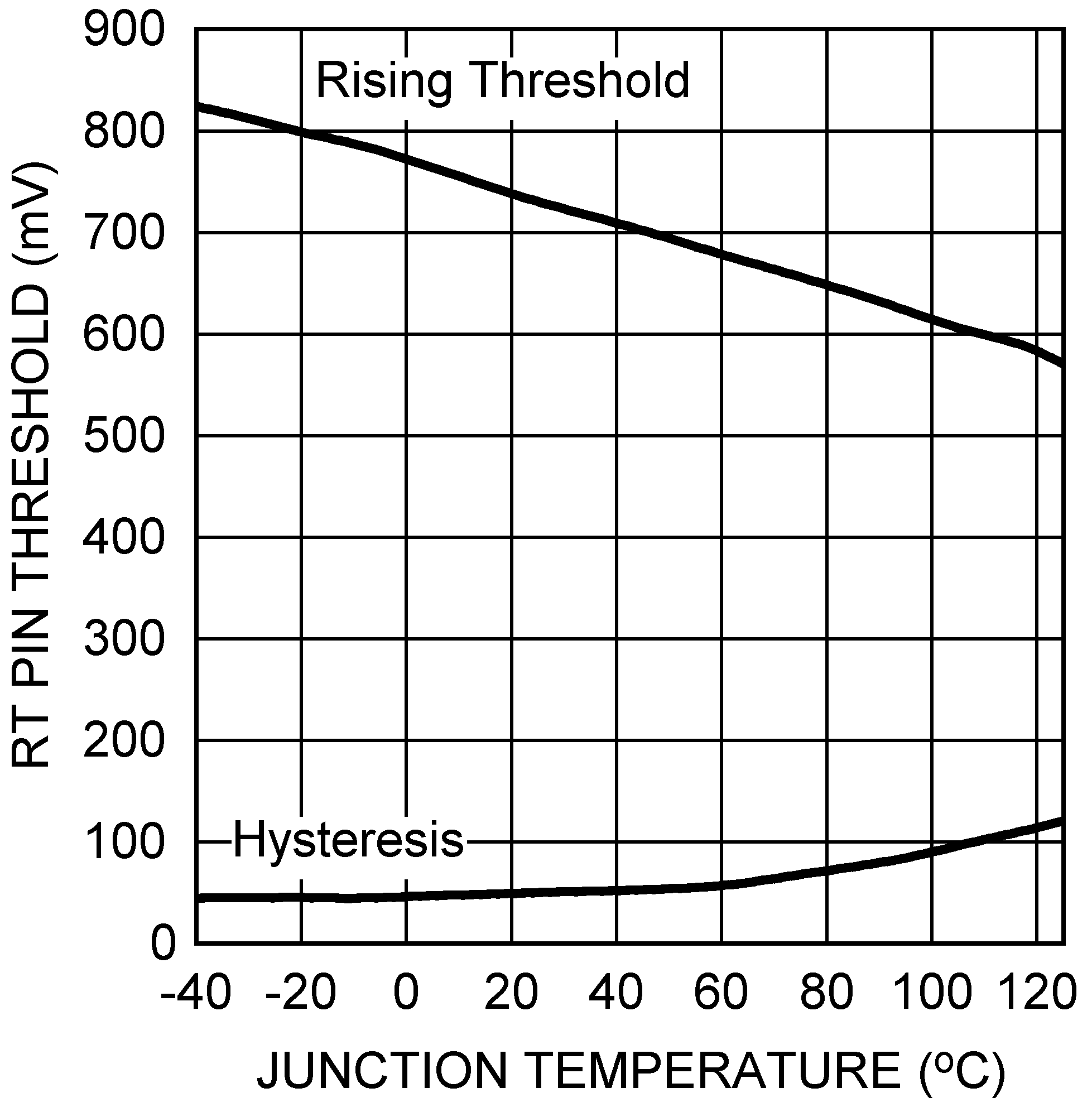
| RTSD | Shutdown Threshold | RT Pin Voltage Rising | 0.73 | V | ||
| RTHYS | Shutdown Threshold Hysteresis | 50 | mV | |||
| ON-TIME | ||||||
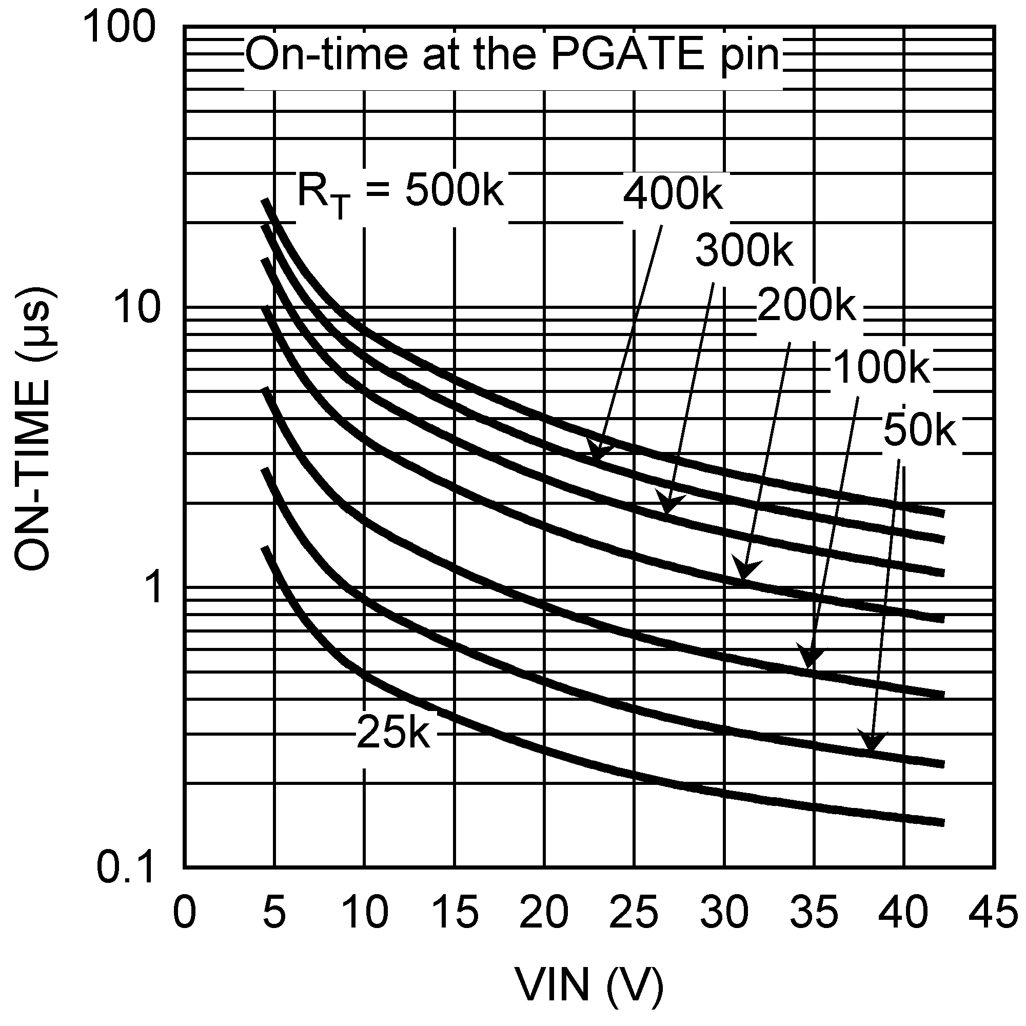
| tON – 1 | On-Time | VIN = 4.5V, RT = 100kΩ | 3.5 | 5 | 7.15 | µs |
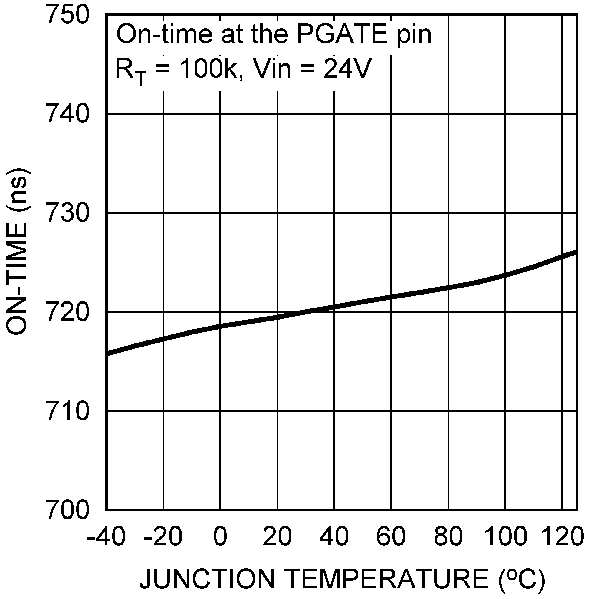
| tON – 2 | VIN = 24V, RT = 100kΩ | 560 | 720 | 870 | ns | |
| tON - 3 | VIN = 42V, RT = 100kΩ | 329 | 415 | 500 | ns | |
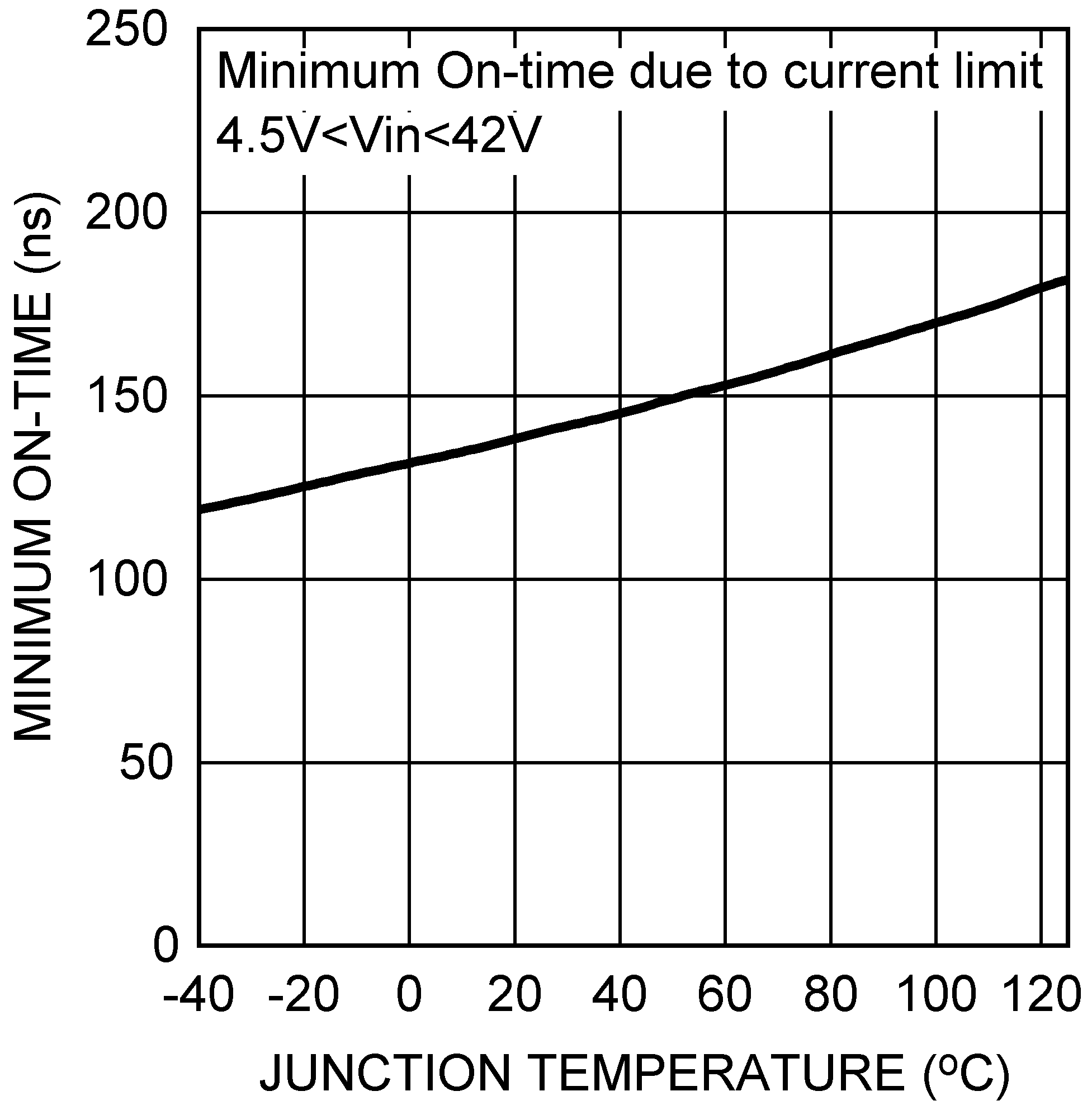
| tON - 4 | Minimum On-Time in Current Limit (4) | VIN = 24V, 25mV Overdrive at ISEN | 55 | 140 | 235 | ns |
| OFF-TIME | ||||||
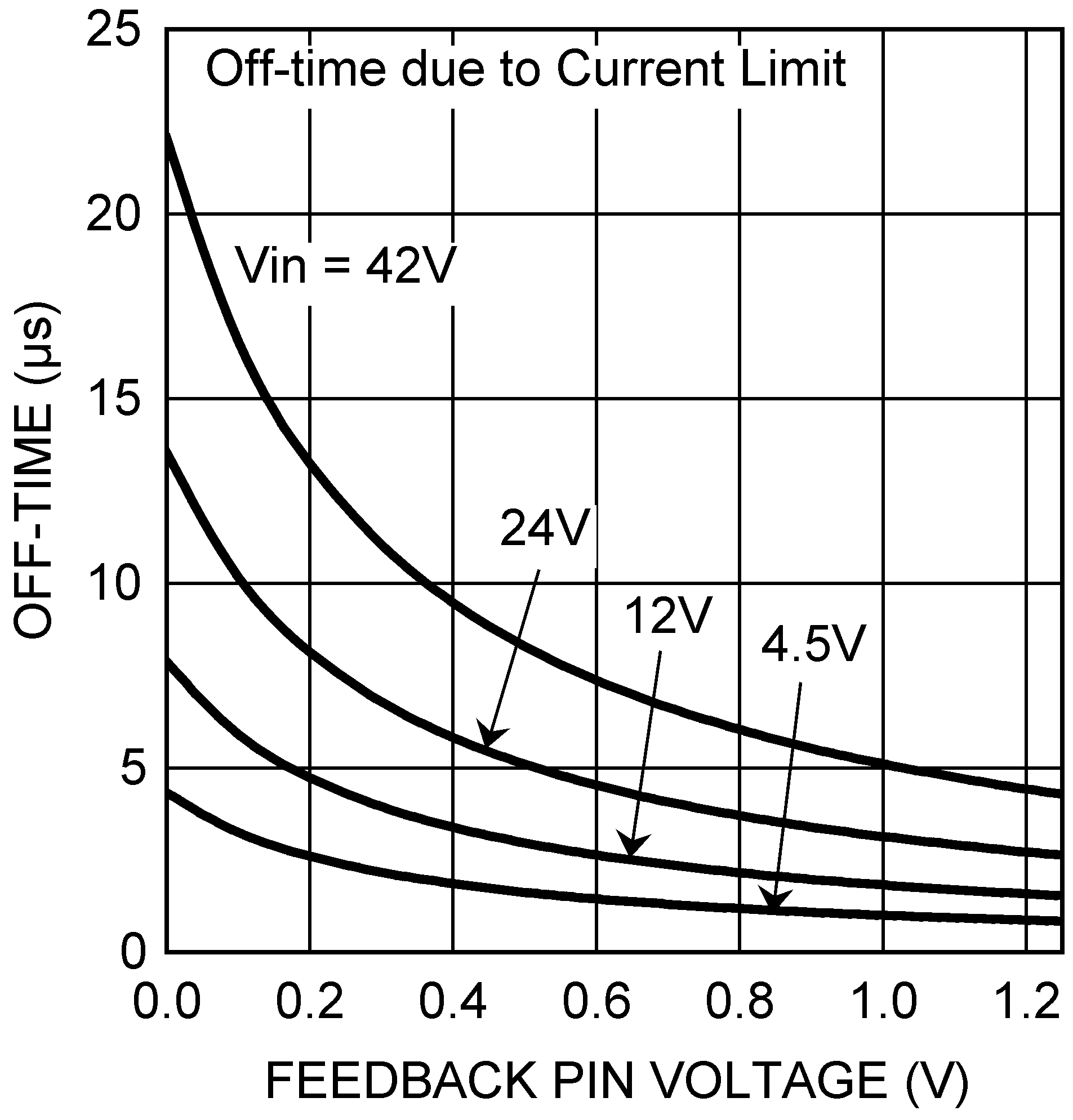
| tOFF(CL1) | Off-Time (Current Limit) (4) | VIN = 12V, VFB = 0V | 5.35 | 7.9 | 10.84 | µs |
| tOFF(CL2) | VIN = 12V, VFB = 1V | 1.42 | 1.9 | 3.03 | µs | |
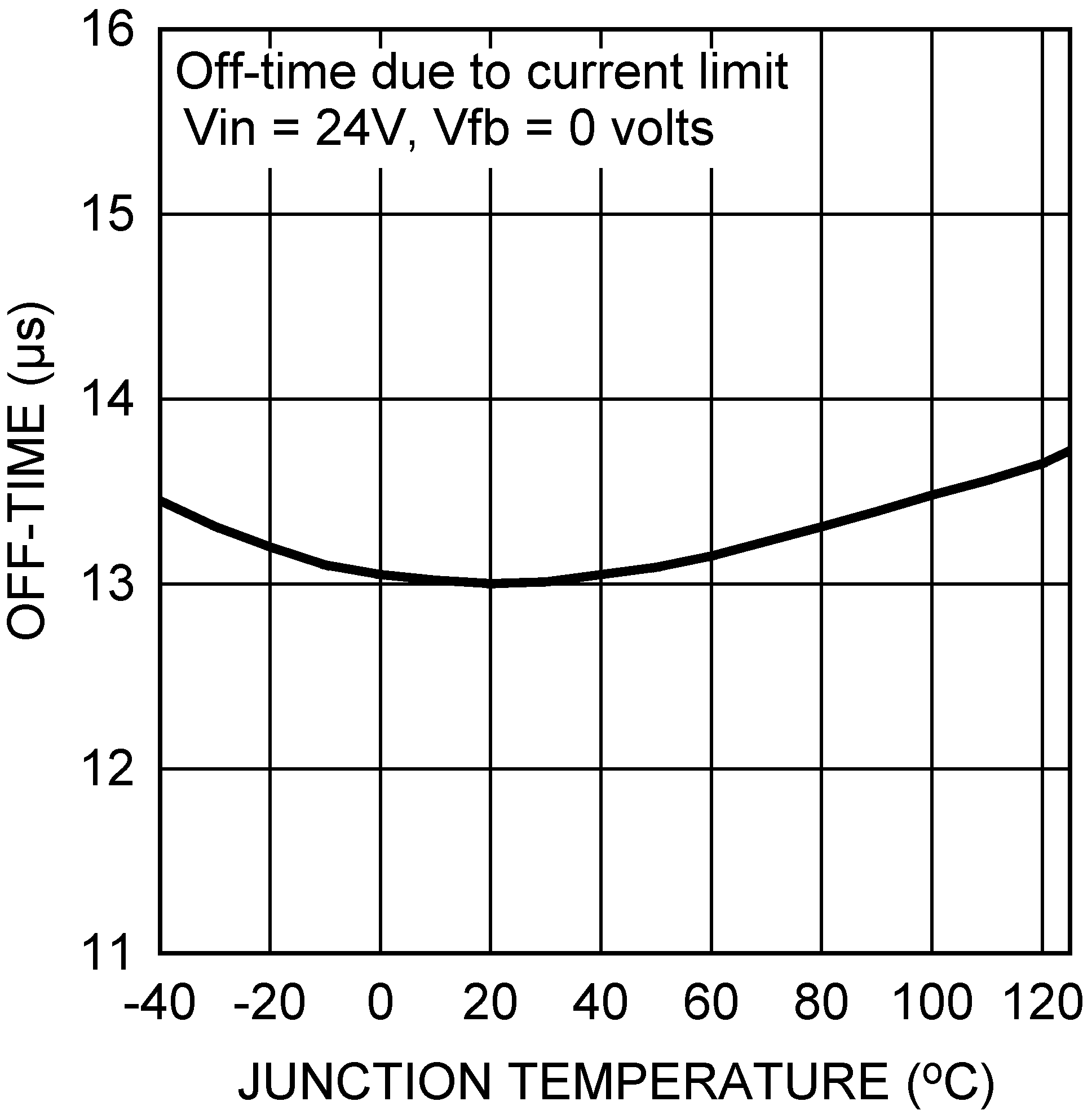
| tOFF(CL3) | VIN = 24V, VFB = 0V | 8.9 | 13 | 17.7 | µs | |
| tOFF(CL4) | VIN = 24V, VFB = 1V | 2.22 | 3.2 | 4.68 | µs | |
| REGULATION AND OVER-VOLTAGE COMPARATORS (FB PIN) | ||||||
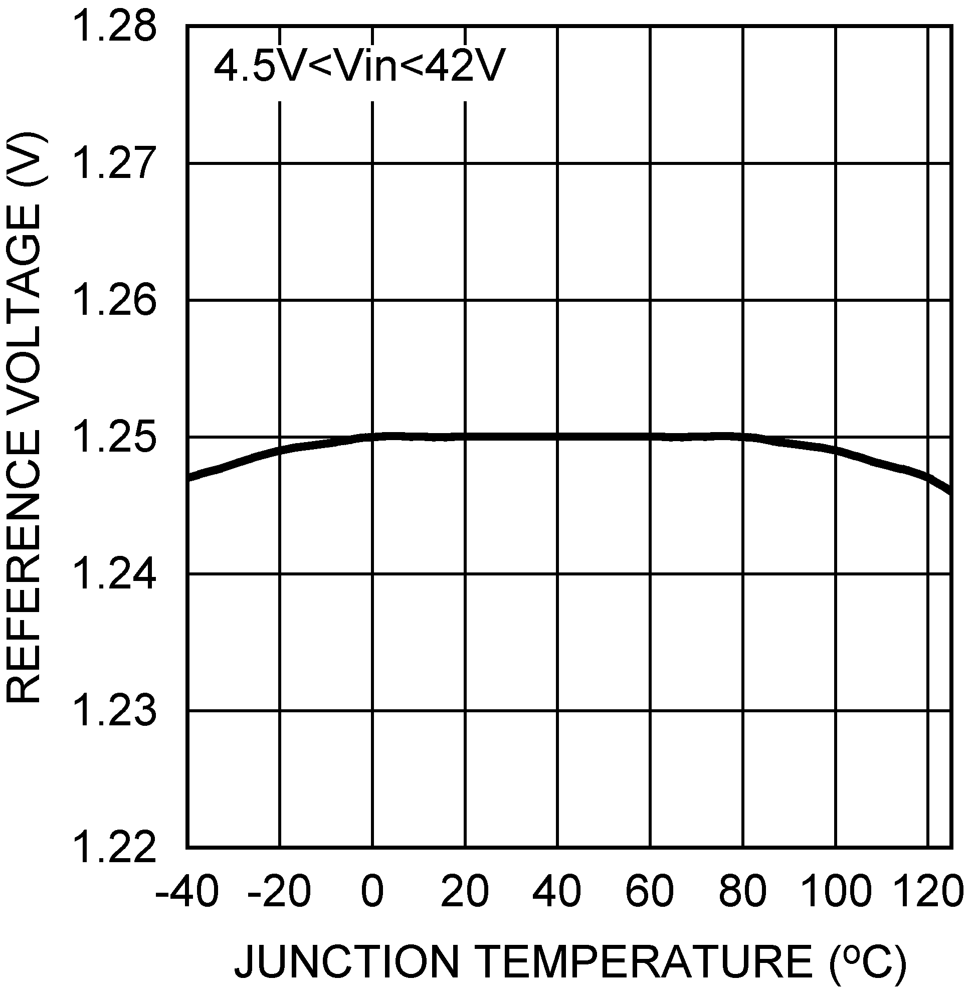
| VREF | FB Regulation Threshold | 1.225 | 1.25 | 1.275 | V | |
| VOV | FB Over-Voltage Threshold | Measured With Respect to VREF | 350 | mV | ||
| IFB | FB Bias Current | 10 | nA | |||
| SOFT-START FUNCTION | ||||||
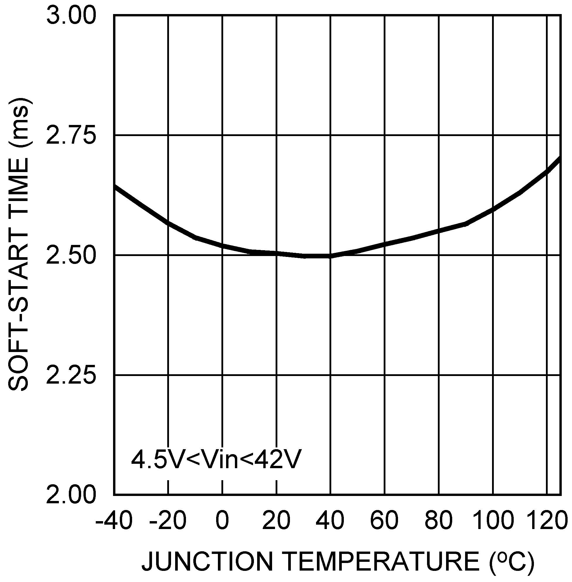
| tSS | Soft-Start Time | 1.4 | 2.5 | 4.3 | ms | |
| THERMAL SHUTDOWN | ||||||
| TSD | Junction Shutdown Temperature | Junction Temperature Rising | 170 | °C | ||
| THYS | Junction Shutdown Hysteresis | 20 | °C | |||
(1) Absolute Maximum Ratings are limits beyond which damage to the device may occur. Operating Ratings are conditions under which operation of the device is intended to be functional. For specifications and test conditions, see the Electrical Characteristics.
(2) VCC provides self bias for the internal gate drive.
(3) Operating current and shutdown current do not include the current in the RT resistor.
(4) The tolerance of the minimum on-time (tON-4) and the current limit off-times (tOFF(CL1) through (tOFF(CL4)) track each other over process and temperature variations. A device which has an on-time at the high end of the range will have an off-time that is at the high end of its range.
(5) All hot and cold limits are specified by correlating the electrical characteristics to process and temperature variations and applying statistical process control.
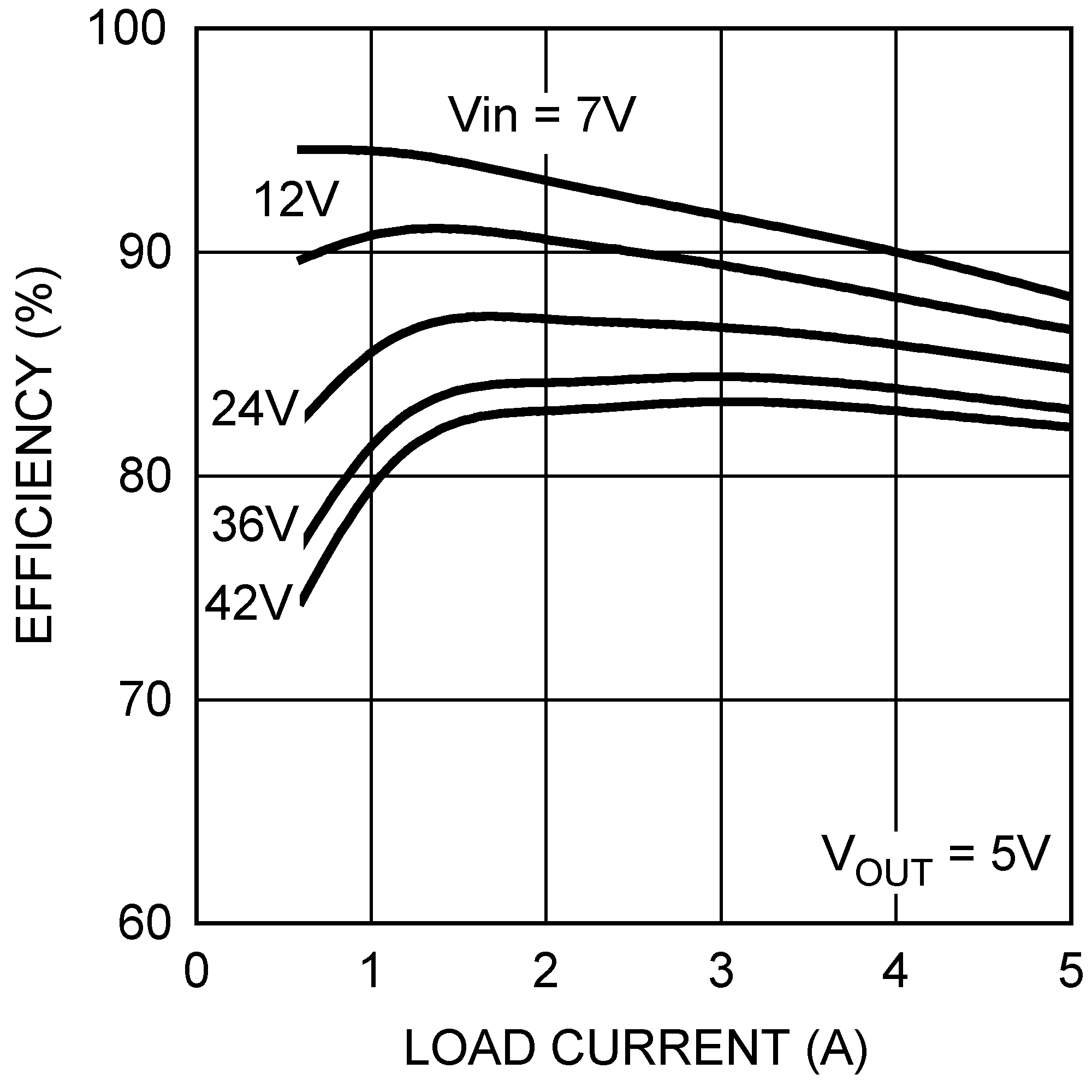
6.7 Typical Characteristics
Unless otherwise specified the following conditions apply: TJ = 25°C, VIN = 24V.