SNVS714F April 2011 – August 2015 LM25117 , LM25117-Q1
PRODUCTION DATA.
- 1 Features
- 2 Applications
- 3 Description
- 4 Revision History
- 5 Pin Configuration and Functions
- 6 Specifications
-
7 Detailed Description
- 7.1 Overview
- 7.2 Functional Block Diagram
- 7.3
Feature Description
- 7.3.1 High Voltage Startup Regulator and VCC Disable
- 7.3.2 UVLO
- 7.3.3 Oscillator And Sync Capability
- 7.3.4 Ramp Generator and Emulated Current Sense
- 7.3.5 Error Amplifier and PWM Comparator
- 7.3.6 Soft-Start
- 7.3.7 Cycle-By-Cycle Current Limit
- 7.3.8 Hiccup Mode Current Limiting
- 7.3.9 HO and LO Drivers
- 7.3.10 Current Monitor
- 7.3.11 Maximum Duty Cycle
- 7.3.12 Thermal Protection
- 7.4 Device Functional Modes
-
8 Application and Implementation
- 8.1 Application Information
- 8.2 Typical Applications
- 8.3
Detailed Design Procedure
- 8.3.1 Feedback Compensation
- 8.3.2 Sub-Harmonic Oscillation
- 8.3.3 Design Requirements
- 8.3.4 Timing Resistor RT
- 8.3.5 Output Inductor LO
- 8.3.6 Diode Emulation Function
- 8.3.7 Current Sense Resistor RS
- 8.3.8 Current Sense Filter RCS and CCS
- 8.3.9 Ramp Resistor RRAMP and Ramp Capacitor CRAMP
- 8.3.10 UVLO Divider RUV2, RUV1 and CFT
- 8.3.11 VCC Disable and External VCC Supply
- 8.3.12 Power Switches QH and QL
- 8.3.13 Snubber Components RSNB and CSNB
- 8.3.14 Bootstrap Capacitor CHB and Bootstrap Diode DHB
- 8.3.15 VCC Capacitor CVCC
- 8.3.16 Output Capacitor CO
- 8.3.17 Input Capacitor CIN
- 8.3.18 VIN Filter RVIN, CVIN
- 8.3.19 Soft-Start Capacitor CSS
- 8.3.20 Restart Capacitor CRES
- 8.3.21 Output Voltage Divider RFB2 and RFB1
- 8.3.22 Loop Compensation Components CCOMP, RCOMP and CHF
- 8.4 Application Curves
- 9 Power Supply Recommendations
- 10Layout
- 11Device and Documentation Support
- 12Mechanical, Packaging, and Orderable Information
Package Options
Mechanical Data (Package|Pins)
Thermal pad, mechanical data (Package|Pins)
Orderable Information
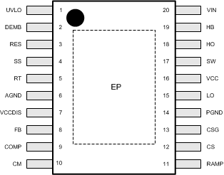
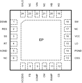
5 Pin Configuration and Functions
PWP Package
20-Pin HTSSOP
Top View

RTW Package
24-Pin WQFN
Top View

Pin Functions
| PIN | TYPE(1) | DESCRIPTION | ||
|---|---|---|---|---|
| HTSSOP NO. | WQFN NO. | NAME | ||
| 1 | 24 | UVLO | I | Undervoltage lockout programming pin. If the UVLO pin voltage is below 0.4V, the regulator is in the shutdown mode with all functions disabled. If the UVLO pin voltage is greater than 0.4V and less than 1.25V, the regulator is in standby mode with the VCC regulator operational, the SS pin grounded, and no switching at the HO and LO outputs. If the UVLO pin voltage is above 1.25 V, the SS pin is allowed to ramp and pulse width modulated gate drive signals are delivered to the HO and LO pins. A 20μA current source is enabled when UVLO exceeds 1.25V and flows through the external UVLO resistors to provide hysteresis. |
| 2 | 1 | DEMB | I | Optional logic input that enables diode emulation when in the low state. In diode emulation mode, the low-side NMOS is latched off for the remainder of the PWM cycle after detecting reverse current flow (current flow from output to ground through the low-side NMOS). When DEMB is high, diode emulation is disabled allowing current to flow in either direction through the low-side NMOS. A 50kΩ pull-down resistor internal to the LM25117 holds DEMB pin low and enables diode emulation if the pin is left floating. |
| 3 | 2 | RES | O | The restart timer pin that configures the hiccup mode current limiting. A capacitor on the RES pin determines the time the controller remains off before automatically restarting. The hiccup mode commences when the controller experiences 256 consecutive PWM cycles of cycle-by-cycle current limiting. After this occurs, an 10μA current source charges the RES pin capacitor to the 1.25V threshold and restarts LM25117. |
| 4 | 3 | SS | I | An external capacitor and an internal 10μA current source set the ramp rate of the error amplifier reference during soft-start. The SS pin is held low when VCC< 4V, UVLO < 1.25V or during thermal shutdown. |
| 5 | 4 | RT | I | The internal oscillator is programmed with a single resistor between RT and the AGND. The recommended maximum oscillator frequency is 750kHz. The internal oscillator can be synchronized to an external clock by coupling a positive pulse into the RT pin through a small coupling capacitor. |
| 6 | 5 | AGND | G | Analog ground. Return for the internal 0.8V voltage reference and analog circuits. |
| 7 | 7 | VCCDIS | I | Optional input that disables the internal VCC regulator. If VCCDIS>1.25V, the internal VCC regulator is disabled. VCCDIS has an internal 500kΩ pull-down resistor to enable the VCC regulator when the pin is left floating. The internal 500kΩ pull-down resistor can be overridden by pulling VCCDIS above 1.25V with a resistor divider connected to an external bias supply. |
| 8 | 8 | FB | I | Feedback. Inverting input of the internal error amplifier. A resistor divider from the output to this pin sets the output voltage level. The regulation threshold at the FB pin is 0.8V. |
| 9 | 9 | COMP | O | Output of the internal error amplifier. The loop compensation network should be connected between this pin and the FB pin. |
| 10 | 10 | CM | O | Current monitor output. Average of the sensed inductor current is provided. Monitor directly between CM and AGND. CM should be left floating when the pin is not used. |
| 11 | 11 | RAMP | I | PWM ramp signal. An external resistor and capacitor connected between the SW pin, the RAMP pin and the AGND pin sets the PWM ramp slope. Proper selection of component values produces a RAMP signal that emulates the AC component of the inductor with a slope proportional to input supply voltage. |
| 12 | 12 | CS | I | Current sense amplifier input. Connect to the high-side of the current sense resistor. |
| 13 | 13 | CSG | I | Kelvin ground connection to the current sense resistor. Connect directly to the low-side of the current sense resistor. |
| 14 | 14 | PGND | G | Power ground return pin for low-side NMOS gate driver. Connect directly to the low-side of the current sense resistor. |
| 15 | 15 | LO | O | Low-side NMOS gate drive output. Connect to the gate of the low-side synchronous NMOS transistor through a short, low inductance path. |
| 16 | 16 | VCC | P/O/I | Bias supply pin. Locally decouple to PGND using a low ESR/ESL capacitor located as close to controller as possible. |
| 17 | 18 | SW | I/O | Switching node of the buck regulator. Connect to the bootstrap capacitor, the source terminal of the high-side NMOS transistor and the drain terminal of the low-side NMOS through a short, low inductance path. |
| 18 | 19 | HO | O | High-side NMOS gate drive output. Connect to the gate of the high-side NMOS transistor through a short, low inductance path. |
| 19 | 20 | HB | P | High-side driver supply for the bootstrap gate drive. Connect to the cathode of the external bootstrap diode and to the bootstrap capacitor. The bootstrap capacitor supplies current to charge the high-side NMOS gate and should be placed as close to controller as possible. |
| 20 | 22 | VIN | P/I | Supply voltage input source for the VCC regulator. |
| EP | EP | EP | - | Exposed pad of the package. Electrically isolated. Should be soldered to the ground plane to reduce thermal resistance. |
| 6 | NC | - | No electrical contact. | |
| 17 | NC | - | No electrical contact. | |
| 21 | NC | - | No electrical contact. | |
| 23 | NC | - | No electrical contact. | |
(1) I = Input, O = Output, G = Ground, P = Power