SNVS714F April 2011 – August 2015 LM25117 , LM25117-Q1
PRODUCTION DATA.
- 1 Features
- 2 Applications
- 3 Description
- 4 Revision History
- 5 Pin Configuration and Functions
- 6 Specifications
-
7 Detailed Description
- 7.1 Overview
- 7.2 Functional Block Diagram
- 7.3
Feature Description
- 7.3.1 High Voltage Startup Regulator and VCC Disable
- 7.3.2 UVLO
- 7.3.3 Oscillator And Sync Capability
- 7.3.4 Ramp Generator and Emulated Current Sense
- 7.3.5 Error Amplifier and PWM Comparator
- 7.3.6 Soft-Start
- 7.3.7 Cycle-By-Cycle Current Limit
- 7.3.8 Hiccup Mode Current Limiting
- 7.3.9 HO and LO Drivers
- 7.3.10 Current Monitor
- 7.3.11 Maximum Duty Cycle
- 7.3.12 Thermal Protection
- 7.4 Device Functional Modes
-
8 Application and Implementation
- 8.1 Application Information
- 8.2 Typical Applications
- 8.3
Detailed Design Procedure
- 8.3.1 Feedback Compensation
- 8.3.2 Sub-Harmonic Oscillation
- 8.3.3 Design Requirements
- 8.3.4 Timing Resistor RT
- 8.3.5 Output Inductor LO
- 8.3.6 Diode Emulation Function
- 8.3.7 Current Sense Resistor RS
- 8.3.8 Current Sense Filter RCS and CCS
- 8.3.9 Ramp Resistor RRAMP and Ramp Capacitor CRAMP
- 8.3.10 UVLO Divider RUV2, RUV1 and CFT
- 8.3.11 VCC Disable and External VCC Supply
- 8.3.12 Power Switches QH and QL
- 8.3.13 Snubber Components RSNB and CSNB
- 8.3.14 Bootstrap Capacitor CHB and Bootstrap Diode DHB
- 8.3.15 VCC Capacitor CVCC
- 8.3.16 Output Capacitor CO
- 8.3.17 Input Capacitor CIN
- 8.3.18 VIN Filter RVIN, CVIN
- 8.3.19 Soft-Start Capacitor CSS
- 8.3.20 Restart Capacitor CRES
- 8.3.21 Output Voltage Divider RFB2 and RFB1
- 8.3.22 Loop Compensation Components CCOMP, RCOMP and CHF
- 8.4 Application Curves
- 9 Power Supply Recommendations
- 10Layout
- 11Device and Documentation Support
- 12Mechanical, Packaging, and Orderable Information
Package Options
Mechanical Data (Package|Pins)
Thermal pad, mechanical data (Package|Pins)
Orderable Information
6 Specifications
6.1 Absolute Maximum Ratings
over operating free-air temperature range (unless otherwise noted)(1)| MIN | MAX | UNIT | ||
|---|---|---|---|---|
| VIN to AGND | -0.3 | 45 | V | |
| SW to AGND | -3.0 | 45 | V | |
| HB to SW | -0.3 | 15 | V | |
| VCC to AGND(2) | -0.3 | 15 | V | |
| HO to SW | -0.3 | HB+0.3 | V | |
| LO to AGND | -0.3 | VCC+0.3 | V | |
| FB, DEMB, RES, VCCDIS, UVLO to AGND | -0.3 | 15 | V | |
| CM, COMP to AGND(3) | -0.3 | 7 | V | |
| SS, RAMP, RT to AGND | -0.3 | 7 | V | |
| CS, CSG, PGND, to AGND | -0.3 | 0.3 | V | |
| Storage temperature, Tstg | -55 | 150 | °C | |
| Junction Temperature | -40 | 150 | °C | |
(1) Stresses beyond those listed under Absolute Maximum Ratings may cause permanent damage to the device. These are stress ratings only, which do not imply functional operation of the device at these or any other conditions beyond those indicated under Recommended Operating Conditions. Exposure to absolute-maximum-rated conditions for extended periods may affect device reliability.
(2) See Application and Implementation when input supply voltage is less than the VCC voltage.
(3) These pins are output pins. As such they are not specified to have an external voltage applied.
6.2 ESD Ratings (LM25117)
| VALUE | UNIT | |||
|---|---|---|---|---|
| V(ESD) | Electrostatic discharge | Human-body model (HBM), per ANSI/ESDA/JEDEC JS-001(1) | ±2000 | V |
| Charged-device model (CDM), per JEDEC specification JESD22- V C101(2) | ±750 | V | ||
(1) JEDEC document JEP155 states that 500-V HBM allows safe manufacturing with a standard ESD control process.
(2) JEDEC document JEP157 states that 250-V CDM allows safe manufacturing with a standard ESD control process.
6.3 ESD Ratings (LM25117-Q1)
| VALUE | UNIT | |||
|---|---|---|---|---|
| V(ESD) | Electrostatic discharge | Human-body model (HBM), per AEC Q100-002(1) | ±2000 | V |
| Charged-device model (CDM), per AEC Q100-011 | ±750 | V | ||
(1) AEC Q100-002 indicates that HBM stressing shall be in accordance with the ANSI/ESDA/JEDEC JS-001 specification.
6.4 Recommended Operating Conditions
over operating free-air temperature range (unless otherwise noted) (1)| MIN | MAX | UNIT | ||
|---|---|---|---|---|
| VIN(2) | 4.5 | 42 | V | |
| VCC | 4.5 | 14 | V | |
| HB to SW | 4.5 | 14 | V | |
| Junction Temperature | -40 | 125 | °C | |
(1) Recommended Operating Conditions are conditions under which operation of the device is intended to be functional, but does not ensure specific performance limits. For specifications and test conditions see .Electrical Characteristics
(2) Minimum VIN operating voltage is defined with VCC supplied by the internal HV startup regulator and no external load on VCC. When VCC is supplied by an external source, minimum VIN operating voltage is 4.5 V.
6.5 Thermal Information
| THERMAL METRIC(1) | LM25117, LM25117-Q1 | UNIT | ||
|---|---|---|---|---|
| PWP (HTSSOP) | RTW (WQFN) | |||
| 20 PINS | 24 PINS | |||
| RθJA | Junction-to-ambient thermal resistance | 40 | 40 | °C/W |
| RθJC(top) | Junction-to-case (top) thermal resistance | 4 | 6 | °C/W |
(1) For more information about traditional and new thermal metrics, see the Semiconductor and IC Package Thermal Metrics application report, SPRA953.
6.6 Electrical Characteristics
Typical limits are for TJ = 25°C only; typical values represent the most likely parametric norm at TJ = 25°C, and are provided for reference purposes only. Minimum and maximum limits apply over the junction temperature range of –40°C to +125°C. Unless otherwise specified, the following conditions apply: VVIN = 24 V, VVCCDIS = 0 V, RT = 25 kΩ, no load on LO & HO.| PARAMETER | TEST CONDITIONS | MIN | TYP | MAX | UNIT | |
|---|---|---|---|---|---|---|
| VIN SUPPLY | ||||||
| IBIAS | VIN Operating Current (1) | VSS = 0V | 4.8 | 6.2 | mA | |
| VSS = 0V, VVCCDIS = 2V | 0.4 | 0.55 | mA | |||
| ISHUTDOWN | VIN Shutdown Current | VSS = 0V, VUVLO = 0V | 16 | 40 | µA | |
| VCC Regulator | ||||||
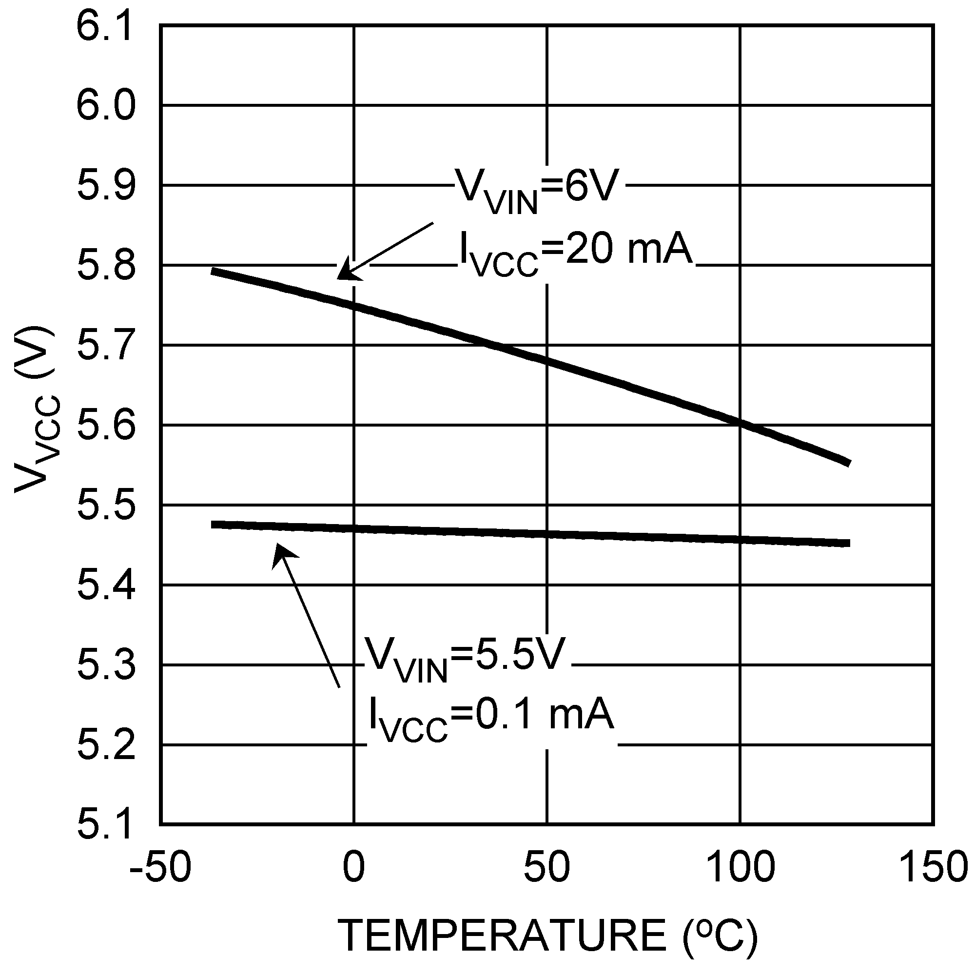
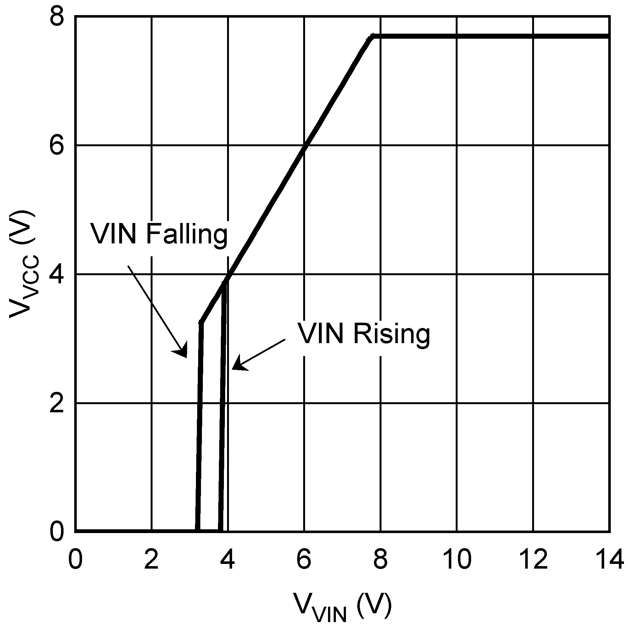
| VCC(REG) | VCC Regulation | No Load | 6.85 | 7.6 | 8.2 | V |
| VCC Dropout (VIN to VCC) | VVIN = 4.5V, No external load | 0.05 | 0.14 | V | ||
| VVIN = 5.0V, ICC = 20mA | 0.4 | 0.5 | V | |||
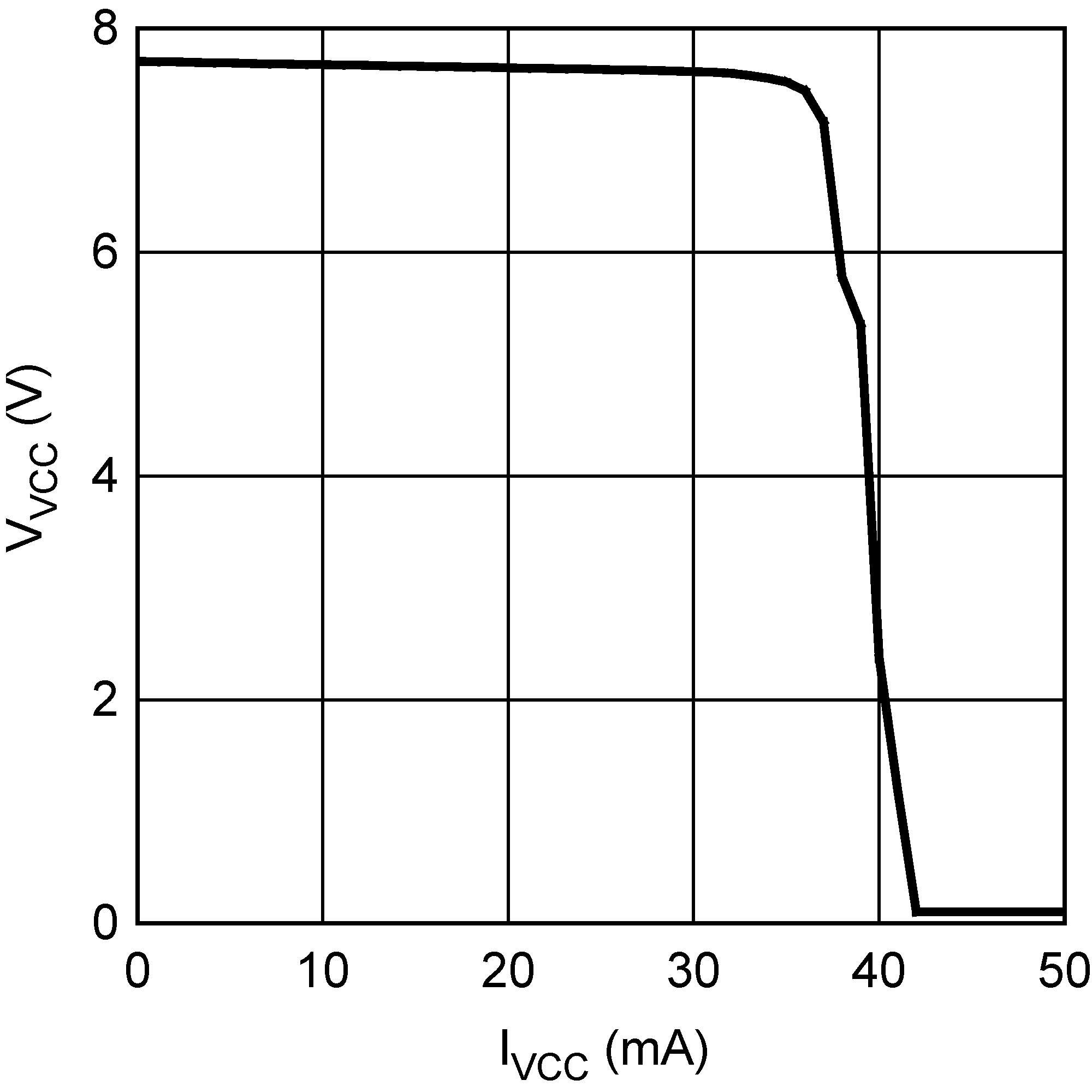
| VCC Sourcing Current Limit | VVCC = 0V | 30 | 42 | mA | ||
| IVCC | VCC Operating Current (1) | VSS = 0V, VVCCDIS = 2V | 4.0 | 5.0 | mA | |
| VSS = 0V, VVCCDIS = 2V, VVCC = 14V | 5.8 | 7.3 | mA | |||
| VCC Under-voltage Threshold | VCC Rising | 3.75 | 4.0 | 4.15 | V | |
| VCC Under-voltage Hysteresis | 0.2 | V | ||||
| VCC Disable | ||||||
| VCCDIS Threshold | VCCDIS Rising | 1.22 | 1.25 | 1.29 | V | |
| VCCDIS Hysteresis | 0.06 | V | ||||
| VCCDIS Input Current | VVCCDIS = 0V | -20 | nA | |||
| VCCDIS Pull-down Resistance | 500 | kΩ | ||||
| UVLO | ||||||
| UVLO Threshold | UVLO Rising | 1.22 | 1.25 | 1.29 | V | |
| UVLO Hysteresis Current | VUVLO = 1.4V | 15 | 20 | 25 | µA | |
| UVLO Shutdown Threshold | UVLO Falling | 0.23 | 0.3 | V | ||
| UVLO Shutdown Hysteresis | 0.1 | V | ||||
| Soft Start | ||||||
| ISS | SS Current Source | VSS = 0V | 7 | 10 | 12 | µA |
| SS Pull-down Resistance | 13 | 24 | Ω | |||
| Error Amplifier | ||||||
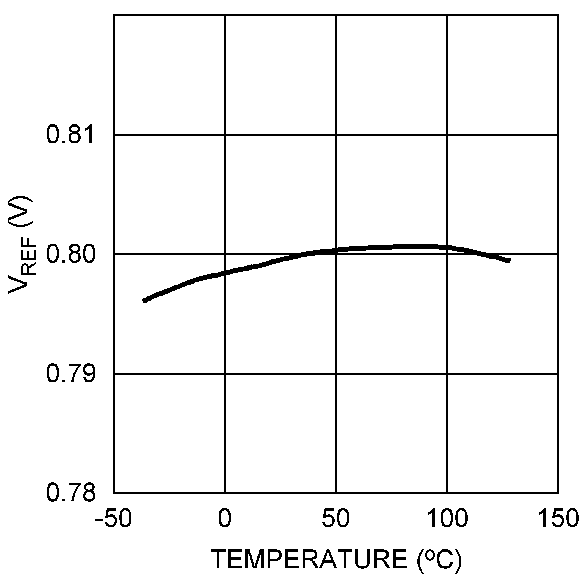
| VREF | FB Reference Voltage | Measured at FB, FB = COMP | 788 | 800 | 812 | mV |
| FB Input Bias Current | VFB = 0.8V | 1 | nA | |||
| VOH | COMP Output High Voltage | ISOURCE = 3mA | 2.8 | V | ||
| VOL | COMP Output Low Voltage | ISINK = 3mA | 0.26 | V | ||
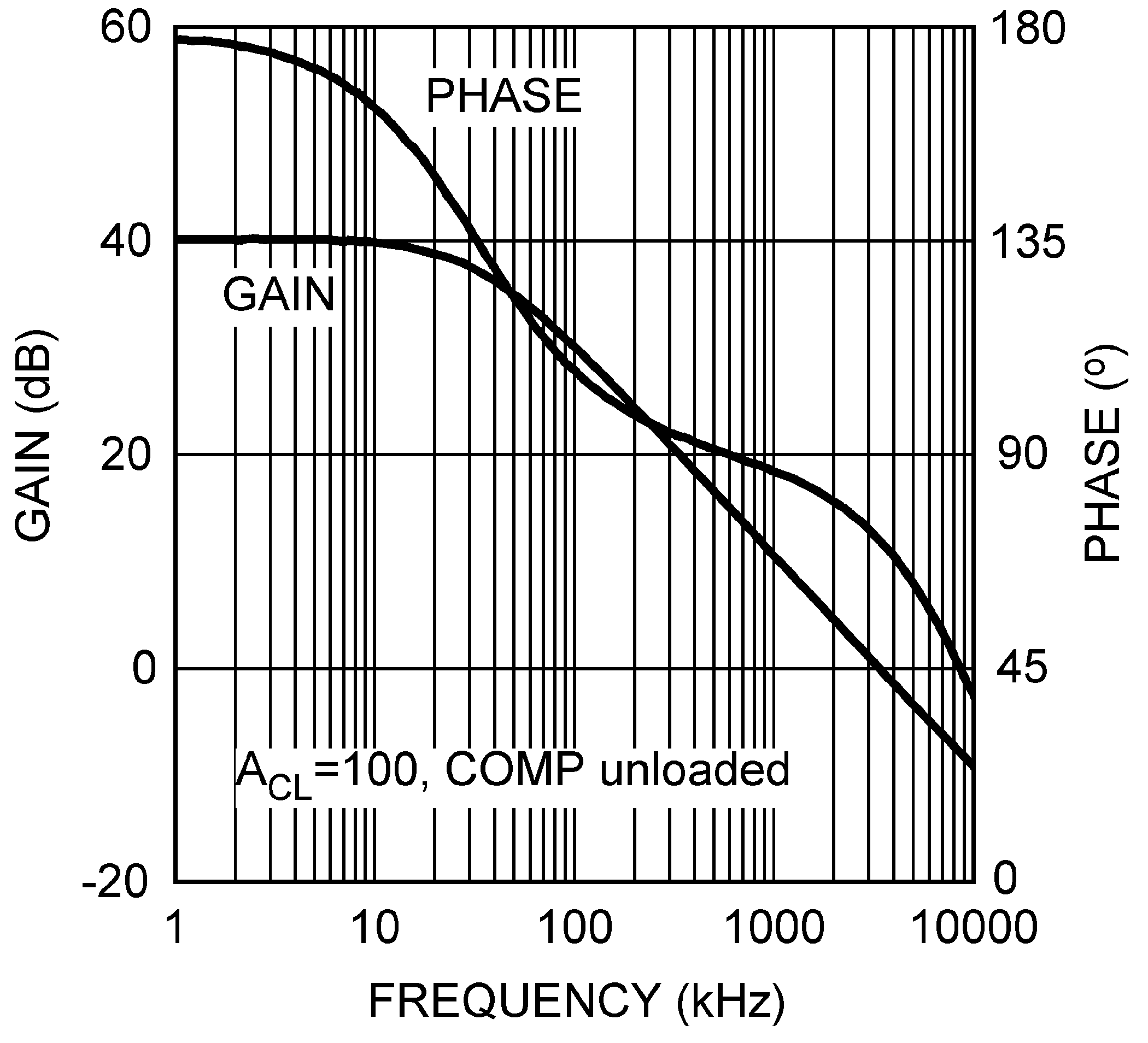
| AOL | DC Gain | 80 | dB | |||
| fBW | Unity Gain Bandwidth | 3 | MHz | |||
| PWM Comparator | ||||||
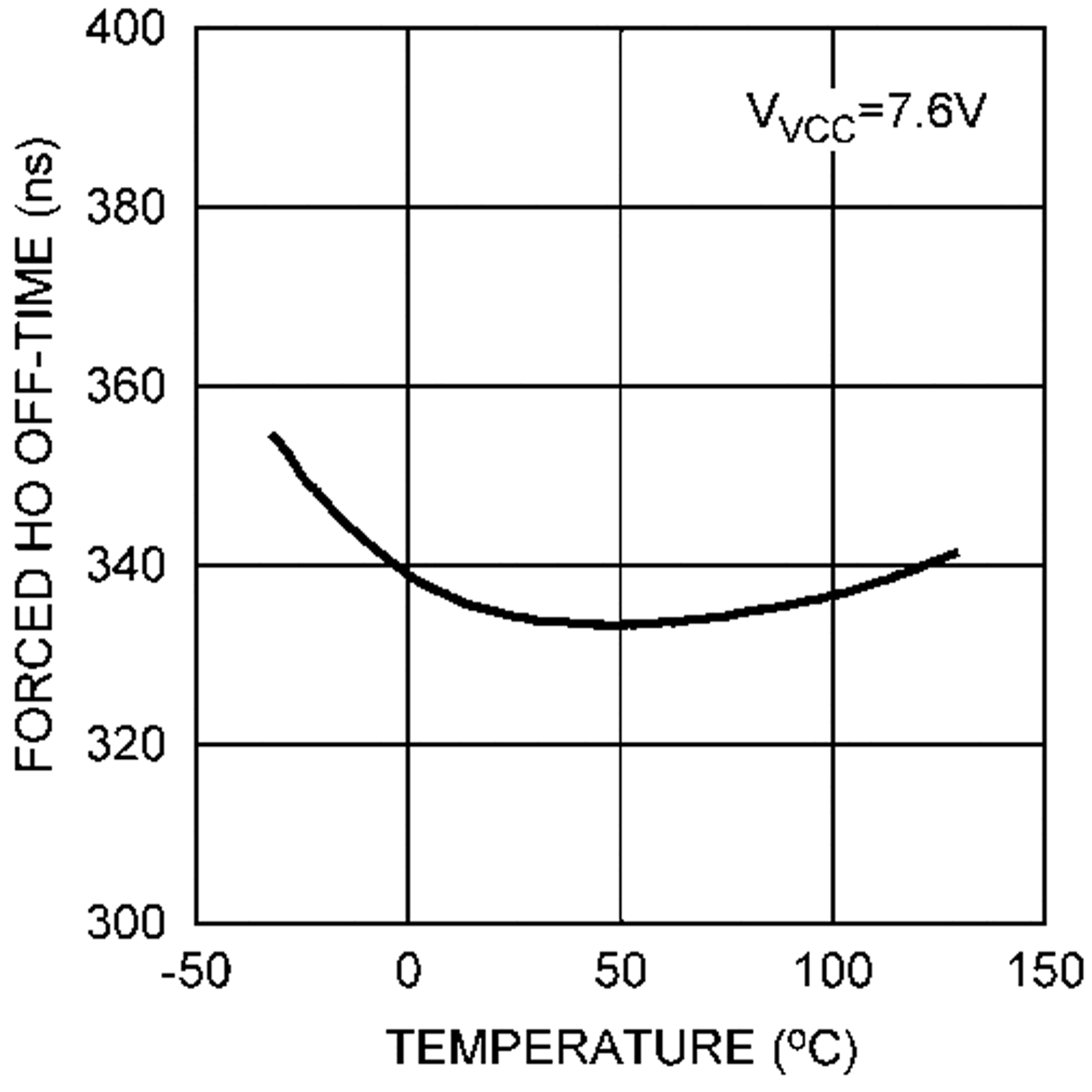
| tHO(OFF) | Forced HO Off-time | 260 | 320 | 440 | ns | |
| tON(MIN) | Minimum HO On-time | VVIN = 42V | 100 | ns | ||
| COMP to PWM comparator offset | 1.2 | V | ||||
| Oscillator | ||||||
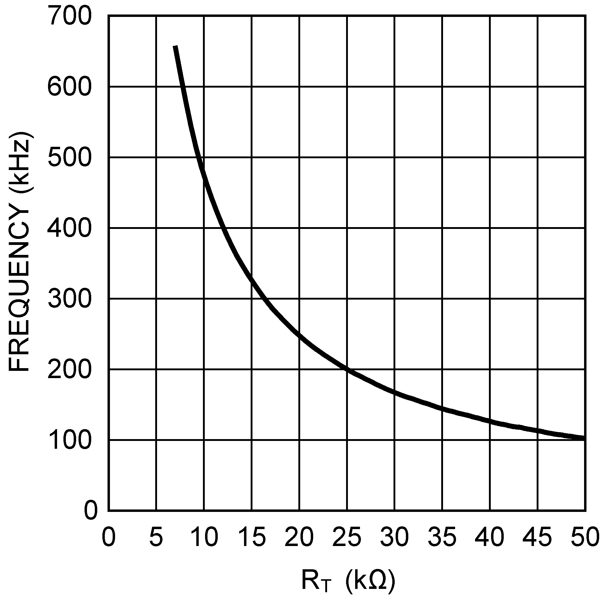
| fSW1 | Frequency 1 | RT = 25kΩ | 180 | 200 | 220 | kHz |
| fSW2 | Frequency 2 | RT = 10kΩ | 430 | 480 | 530 | kHz |
| RT Output Voltage | 1.25 | V | ||||
| RT Sync Positive Threshold | 2.6 | 3.2 | 3.95 | V | ||
| Sync Pulse Width | 100 | ns | ||||
| Current Limit | ||||||
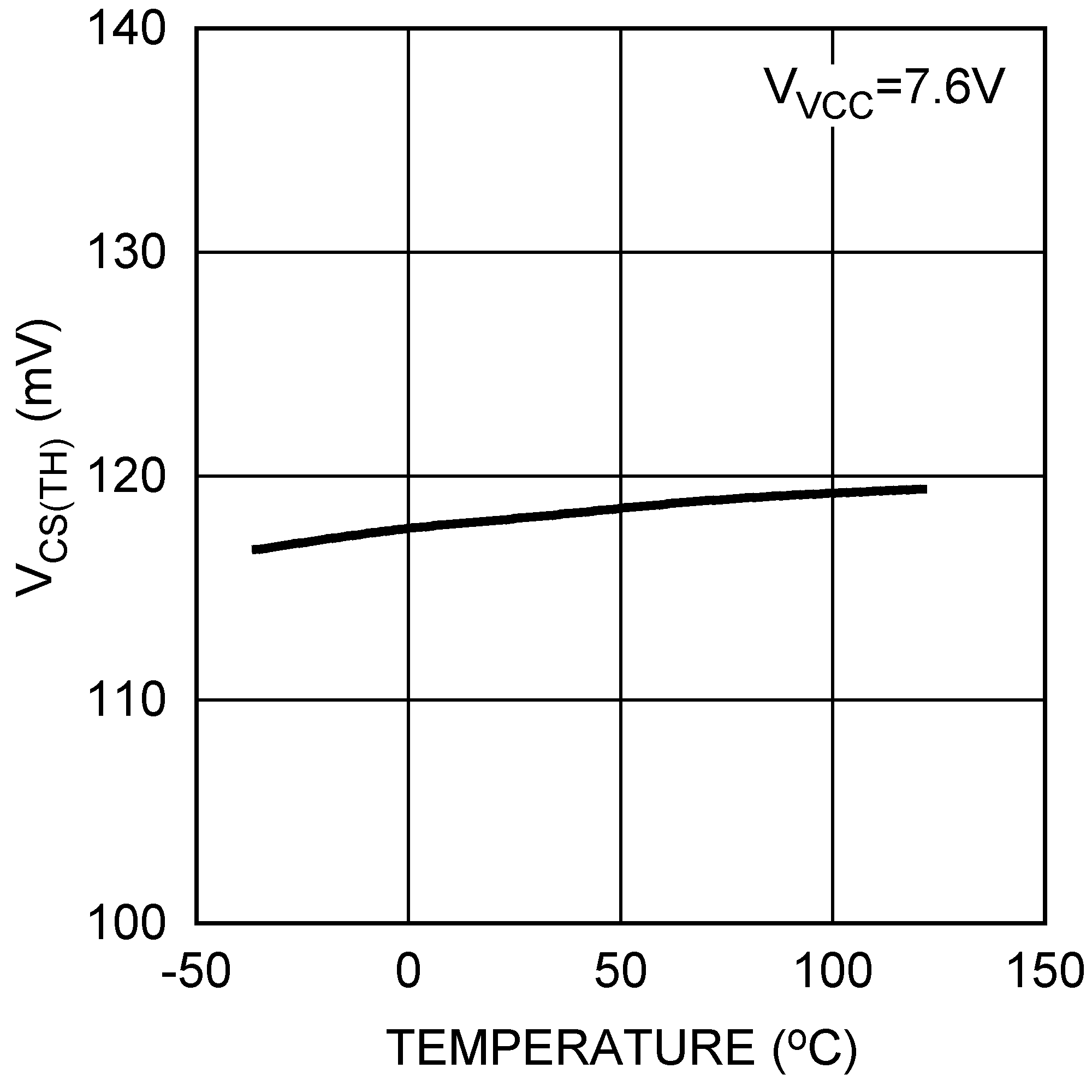
| VCS(TH) | Cycle-by-cycle Sense Voltage Threshold | VRAMP = 0, CSG to CS | 106 | 120 | 135 | mV |
| CS Input Bias Current | VCS = 0V | -100 | -66 | µA | ||
| CSG Input Bias Current | VCSG = 0V | -100 | -66 | µA | ||
| Current Sense Amplifier Gain | 10 | V/V | ||||
| Hiccup Mode Fault Timer | 256 | Cycles | ||||
| RES | ||||||
| IRES | RES Current Source | 10 | µA | |||
| VRES | RES Threshold | RES Rising | 1.22 | 1.25 | 1.285 | V |
| Diode Emulation | ||||||
| VIL | DEMB Input Low Threshold | 2.0 | 1.65 | V | ||
| VIH | DEMB Input High Threshold | 2.95 | 2.5 | V | ||
| SW Zero Cross Threshold | -5 | mV | ||||
| DEMB Input Pull-down Resistance | 50 | kΩ | ||||
| Current Monitor | ||||||
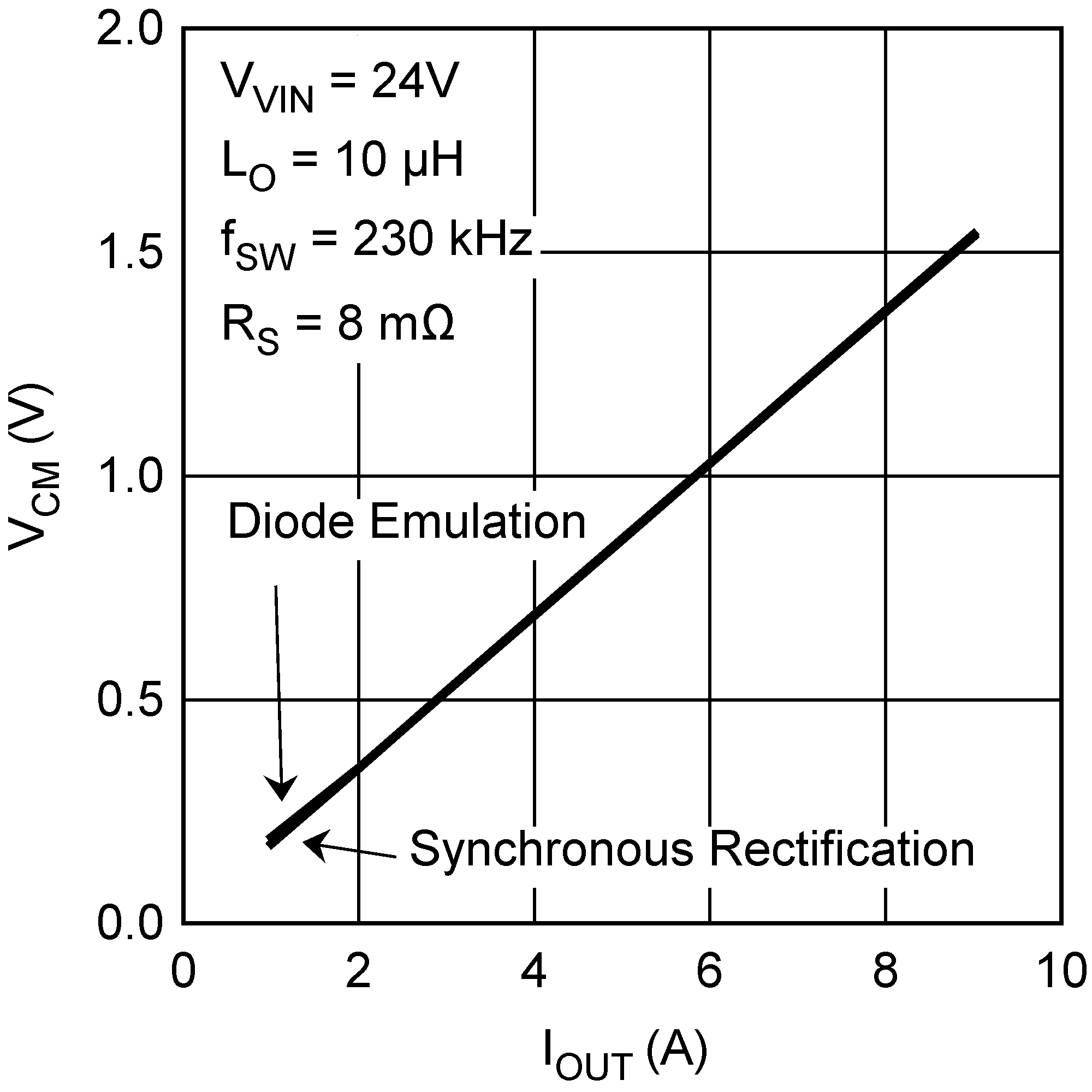
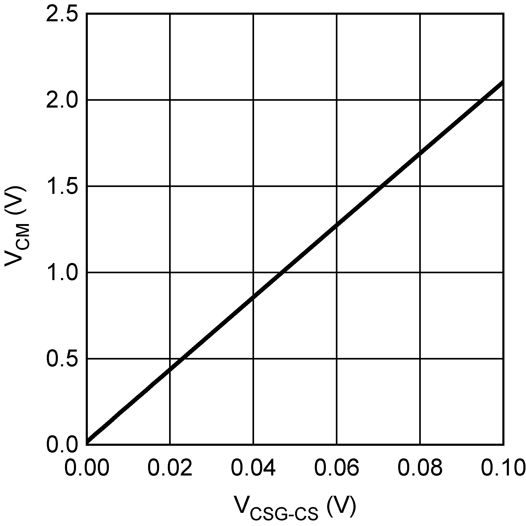
| Current Monitor Amplifier Gain | CS to CM | 17.5 | 20.5 | 23.5 | V/V | |
| Current Monitor Amplifier Gain | Drift over Temperature | -2 | 0 | +2 | % | |
| Zero Input Offset | 25 | 120 | mV | |||
| HO Gate Driver | ||||||
| VOHH | HO High-state Voltage Drop | IHO = –100mA, VOHH = VHB - VHO | 0.17 | 0.3 | V | |
| VOLH | HO Low-state Voltage Drop | IHO = 100mA, VOLH = VHO - VSW | 0.1 | 0.2 | V | |
| HO Rise Time | C-load = 1000pF (2) | 6 | ns | |||
| HO Fall Time | C-load = 1000pF (2) | 5 | ns | |||
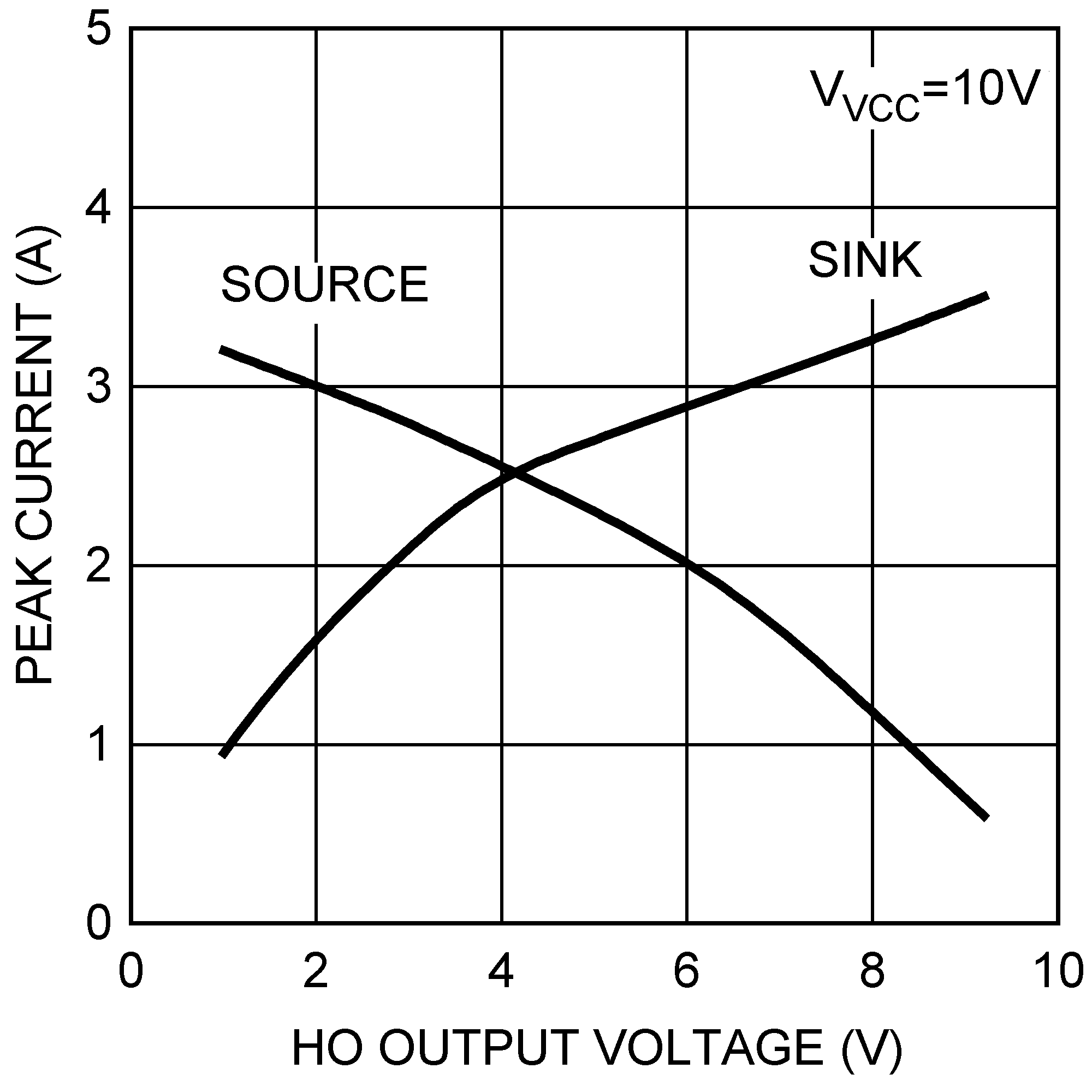
| IOHH | Peak HO Source Current | VHO = 0V, SW = 0V, HB = 7.6V | 2.2 | A | ||
| IOLH | Peak HO Sink Current | VHO = VHB = 7.6V | 3.3 | A | ||
| HB to SW Under-voltage | 2.56 | 2.9 | 3.32 | V | ||
| HB DC Bias Current | HB - SW = 7.6V | 65 | 100 | µA | ||
| LO Gate Driver | ||||||
| VOHL | LO High-state Voltage Drop | ILO = –100mA, VOHL = VCC-VLO | 0.17 | 0.27 | V | |
| VOLL | LO Low-state Voltage Drop | ILO = 100mA, VOLL = VLO | 0.1 | 0.2 | V | |
| LO Rise Time | C-load = 1000pF (2) | 6 | ns | |||
| LO Fall Time | C-load = 1000pF (2) | 5 | ns | |||
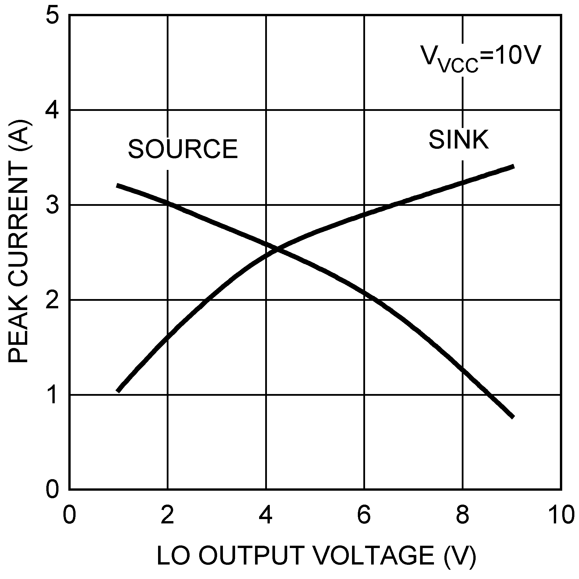
| IOHL | Peak LO Source Current | VLO = 0V | 2.5 | A | ||
| IOLL | Peak LO Sink Current | VLO = 7.6V | 3.3 | A | ||
| Thermal | ||||||
| TSD | Thermal Shutdown | Temperature Rising | 165 | °C | ||
| Thermal Shutdown Hysteresis | 25 | °C | ||||
(1) Operating current does not include the current into the RT resistor.
(2) High and low reference are 80% and 20% of the pulse amplitude respectively.
6.7 Switching Characteristics
over operating free-air temperature range (unless otherwise noted)| PARAMETER | TEST CONDITIONS | MIN | TYP | MAX | UNIT | |
|---|---|---|---|---|---|---|
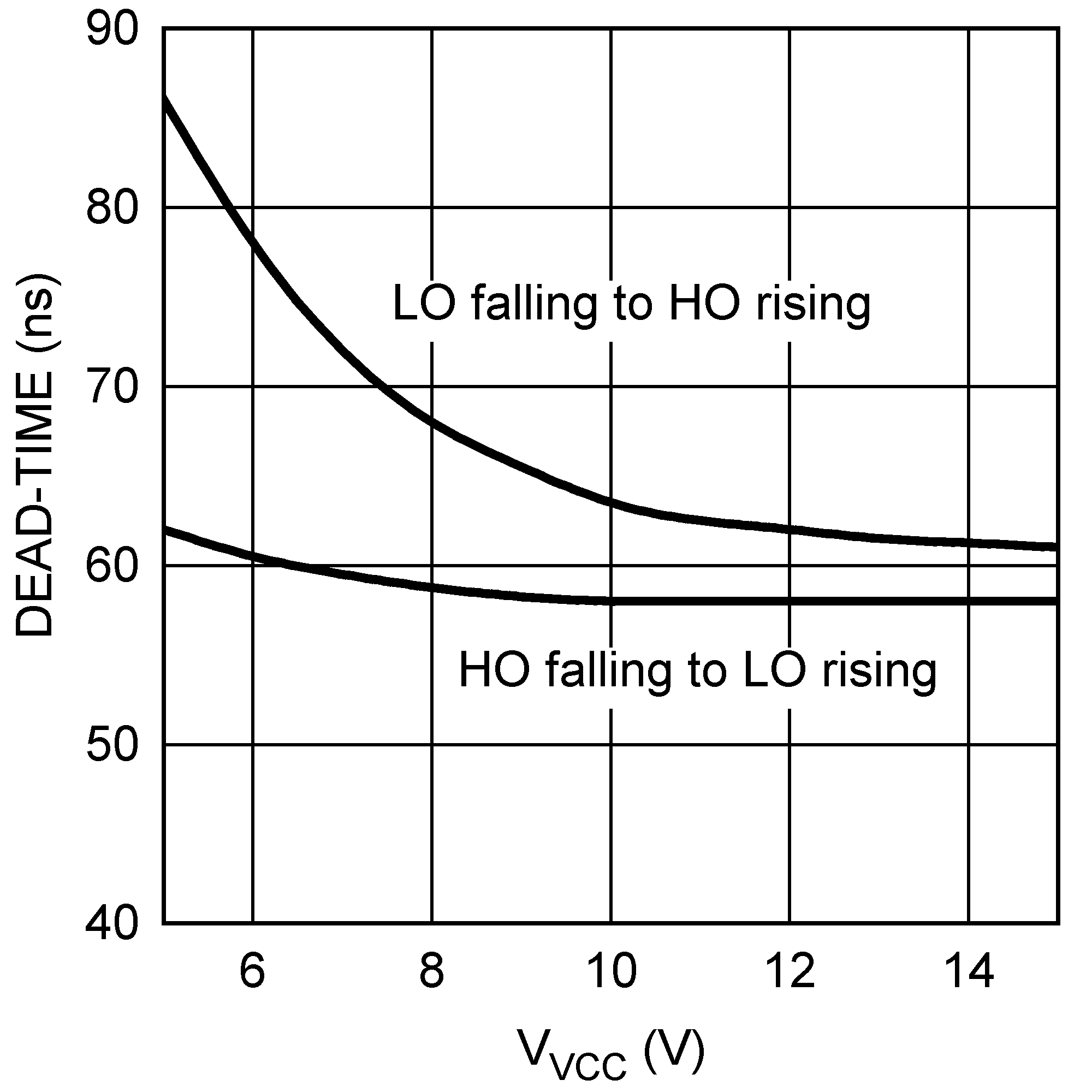
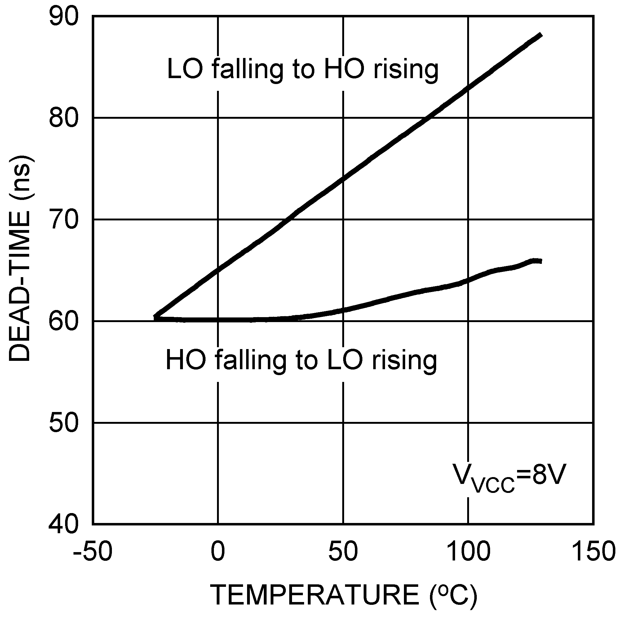
| TDLH | LO fall to HO rise delay | No load | 72 | ns | ||
| TDHL | HO fall to LO rise delay | 71 | ns | |||
6.8 Typical Characteristics
