SNVS124G November   1999  – March 2023 LM2596

PRODUCTION DATA  

  1. Features
  2. Applications
  3. Description
  4. Revision History
  5. Description (continued)
  6. Pin Configuration and Functions
  7. Specifications
    1. 7.1  Absolute Maximum Ratings
    2. 7.2  ESD Ratings
    3. 7.3  Operating Conditions
    4. 7.4  Thermal Information
    5. 7.5  Electrical Characteristics – 3.3-V Version
    6. 7.6  Electrical Characteristics – 5-V Version
    7. 7.7  Electrical Characteristics – 12-V Version
    8. 7.8  Electrical Characteristics – Adjustable Voltage Version
    9. 7.9  Electrical Characteristics – All Output Voltage Versions
    10. 7.10 Typical Characteristics
  8. Detailed Description
    1. 8.1 Overview
    2. 8.2 Functional Block Diagram
    3. 8.3 Feature Description
      1. 8.3.1 Delayed Start-Up
      2. 8.3.2 Undervoltage Lockout
      3. 8.3.3 Inverting Regulator
      4. 8.3.4 Inverting Regulator Shutdown Methods
    4. 8.4 Device Functional Modes
      1. 8.4.1 Discontinuous Mode Operation
  9. Application and Implementation
    1. 9.1 Application Information
      1. 9.1.1 Input Capacitor (CIN)
      2. 9.1.2 Feedforward Capacitor (CFF)
      3. 9.1.3 Output Capacitor (COUT)
      4. 9.1.4 Catch Diode
      5. 9.1.5 Inductor Selection
      6. 9.1.6 Output Voltage Ripple and Transients
      7. 9.1.7 Open-Core Inductors
    2. 9.2 Typical Applications
      1. 9.2.1 LM2596 Fixed Output Series Buck Regulator
        1. 9.2.1.1 Design Requirements
        2. 9.2.1.2 Detailed Design Procedure
          1. 9.2.1.2.1 Custom Design with WEBENCH® Tools
          2. 9.2.1.2.2 Inductor Selection (L1)
          3. 9.2.1.2.3 Output Capacitor Selection (COUT)
          4. 9.2.1.2.4 Catch Diode Selection (D1)
          5. 9.2.1.2.5 Input Capacitor (CIN)
        3. 9.2.1.3 Application Curves
      2. 9.2.2 LM2596 Adjustable Output Series Buck Regulator
        1. 9.2.2.1 Design Requirements
        2. 9.2.2.2 Detailed Design Procedure
          1. 9.2.2.2.1 Programming Output Voltage
          2. 9.2.2.2.2 Inductor Selection (L1)
          3. 9.2.2.2.3 Output Capacitor Selection (COUT)
          4. 9.2.2.2.4 Feedforward Capacitor (CFF)
          5. 9.2.2.2.5 Catch Diode Selection (D1)
          6. 9.2.2.2.6 Input Capacitor (CIN)
        3. 9.2.2.3 Application Curves
    3. 9.3 Power Supply Recommendations
    4. 9.4 Layout
      1. 9.4.1 Layout Guidelines
      2. 9.4.2 Layout Examples
      3. 9.4.3 Thermal Considerations
  10. 10Device and Documentation Support
    1. 10.1 Device Support
      1. 10.1.1 Third-Party Products Disclaimer
      2. 10.1.2 Development Support
        1. 10.1.2.1 Custom Design with WEBENCH® Tools
    2. 10.2 Receiving Notification of Documentation Updates
    3. 10.3 Support Resources
    4. 10.4 Trademarks
    5. 10.5 Electrostatic Discharge Caution
    6. 10.6 Glossary
  11. 11Mechanical, Packaging, and Orderable Information

Package Options

Refer to the PDF data sheet for device specific package drawings

Mechanical Data (Package|Pins)
  • NDH|5
  • NEB|5
  • KTT|5
Thermal pad, mechanical data (Package|Pins)
Orderable Information

Catch Diode

Buck regulators require a diode to provide a return path for the inductor current when the switch turns off. This must be a fast diode and must be placed close to the LM2596 using short leads and short printed-circuit traces.

Because of their very fast switching speed and low forward voltage drop, Schottky diodes provide the best performance, especially in low output voltage applications (5 V and lower). Ultra-fast recovery, or high-efficiency rectifiers are also a good choice, but some types with an abrupt turnoff characteristic can cause instability or EMI problems. Ultra-fast recovery diodes typically have reverse recovery times of 50 ns or less. Rectifiers such as the 1N5400 series are much too slow and must not be used.
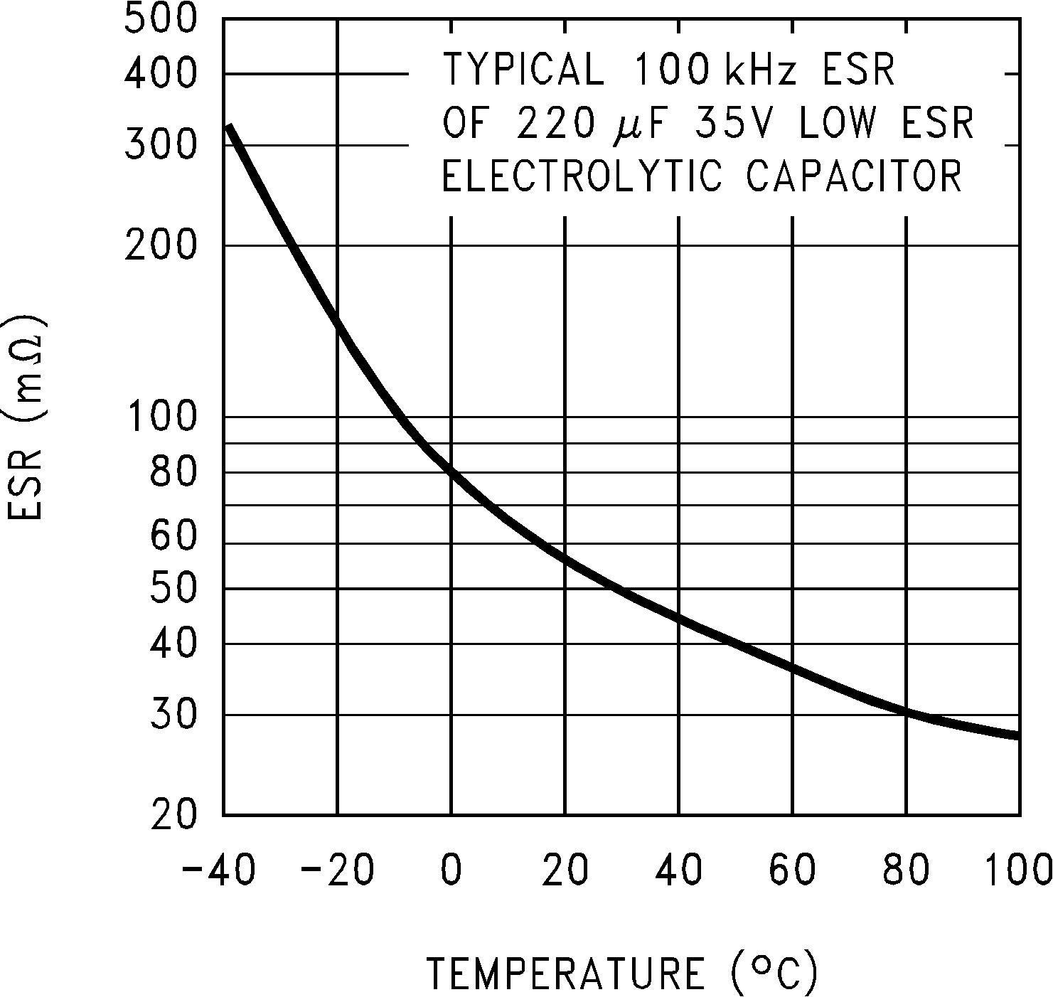
GUID-C98F3A40-2FAF-4382-A9AD-A0118387CDA2-low.pngFigure 9-3 Capacitor ESR Change versus Temperature