SNVS615K January 2010 – February 2018 LM27402
PRODUCTION DATA.
- 1 Features
- 2 Applications
- 3 Description
- 4 Revision History
- 5 Pin Configuration and Functions
- 6 Specifications
-
7 Detailed Description
- 7.1 Overview
- 7.2 Functional Block Diagram
- 7.3
Feature Description
- 7.3.1 Wide Input Voltage Range
- 7.3.2 UVLO
- 7.3.3 Precision Enable
- 7.3.4 Soft-Start and Voltage Tracking
- 7.3.5 Output Voltage Setpoint and Accuracy
- 7.3.6 Voltage-Mode Control
- 7.3.7 Power Good
- 7.3.8 Inductor-DCR-Based Overcurrent Protection
- 7.3.9 Current Sensing
- 7.3.10 Power MOSFET Gate Drivers
- 7.3.11 Pre-Bias Start-up
- 7.4 Device Functional Modes
-
8 Application and Implementation
- 8.1
Application Information
- 8.1.1 Converter Design
- 8.1.2 Inductor Selection (L)
- 8.1.3 Output Capacitor Selection (COUT)
- 8.1.4 Input Capacitor Selection (CIN)
- 8.1.5 Using Precision Enable
- 8.1.6 Setting the Soft-Start Time
- 8.1.7 Tracking
- 8.1.8 Setting the Switching Frequency
- 8.1.9 Setting the Current Limit Threshold
- 8.1.10 Control Loop Compensation
- 8.1.11 MOSFET Gate Drivers
- 8.1.12 Power Loss and Efficiency Calculations
- 8.2 Typical Applications
- 8.1
Application Information
- 9 Power Supply Recommendations
- 10Layout
- 11Device and Documentation Support
- 12Mechanical, Packaging, and Orderable Information
Package Options
Mechanical Data (Package|Pins)
Thermal pad, mechanical data (Package|Pins)
Orderable Information
8.1.7 Tracking
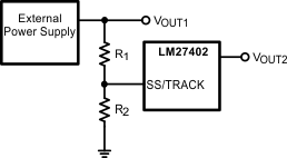
The SS/TRACK pin also functions as a tracking pin when external power supply tracking is needed. Tracking is achieved by simply dividing down the external supply voltage with a simple resistor network shown in Figure 30. With the correct resistor divider configuration, the LM27402 can track an external voltage source to obtain a coincident or ratiometric start-up behavior.
 Figure 30. Tracking an External Power Supply
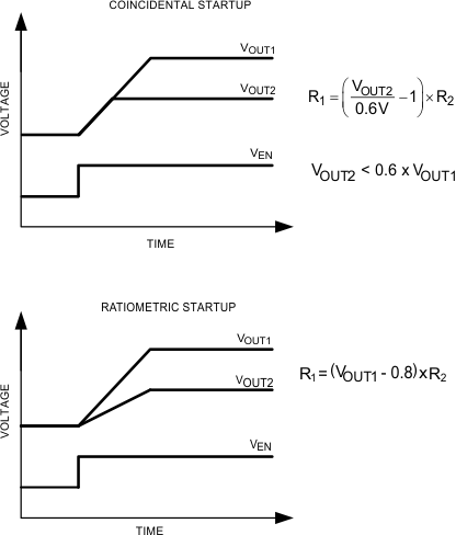
Because the soft-start charging current ISS is sourced from the SS/TRACK pin, the size of R2 must be less than 10 kΩ to minimize errors in the tracking output. Once a value for R2 is selected, calculate the value for R1 using the appropriate equation in Figure 31 to give the desired start-up sequence. Figure 31 shows two common start-up sequences; the upper waveform shows a coincidental start-up while the lower waveform illustrates a ratiometric start-up. A coincidental configuration provides a robust start-up sequence for certain applications because it avoids turning on any parasitic conduction paths that may exist between loads. A ratiometric configuration is preferred in applications where both supplies need to be at the final steady-state voltage at the same time.
 Figure 31. Tracking Start-up Sequences
Similar to the soft-start function, the fastest possible startup time is 1.28 ms regardless of the rise time of the tracking voltage. When using the track feature, the final voltage seen by the SS/TRACK pin should exceed 0.8 V to provide sufficient overdrive and transient immunity.