SNAS555D June 2000 – December 2016 LM2907-N , LM2917-N
PRODUCTION DATA.
- 1 Features
- 2 Applications
- 3 Description
- 4 Revision History
- 5 Description (continued)
- 6 Pin Configuration and Functions
- 7 Specifications
- 8 Parameter Measurement Information
- 9 Detailed Description
-
10Application and Implementation
- 10.1 Application Information
- 10.2
Typical Applications
- 10.2.1 Minimum Component Tachometer
- 10.2.2
Other Application Circuits
- 10.2.2.1 Variable Reluctance Magnetic Pickup Buffer Circuits
- 10.2.2.2 Finger Touch or Contact Switch
- 10.2.2.3 Over-Speed Latch
- 10.2.2.4 Frequency Switch Applications
- 10.2.2.5 Anti-Skid Circuits
- 10.2.2.6 Changing the Output Voltage for an Input Frequency of Zero
- 10.2.2.7 Changing Tachometer Gain Curve or Clamping the Minimum Output Voltage
- 11Power Supply Recommendations
- 12Layout
- 13Device and Documentation Support
- 14Mechanical, Packaging, and Orderable Information
Package Options
Mechanical Data (Package|Pins)
Thermal pad, mechanical data (Package|Pins)
Orderable Information
1 Features
- Ground Referenced Tachometer Input Interfaces Directly With Variable Reluctance Magnetic Pickups
- Op Amp Has Floating Transistor Output
- 50-mA Sink or Source to Operate Relays, Solenoids, Meters, or LEDs
- Frequency Doubling For Low Ripple
- Tachometer Has Built-In Hysteresis With Either Differential Input or Ground Referenced Input
- ±0.3% Linearity (Typical)
- Ground-Referenced Tachometer is Fully Protected From Damage Due to Swings Above VCC and Below Ground
- Output Swings to Ground For Zero Frequency Input
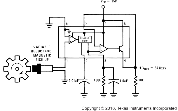
- Easy to Use; VOUT = fIN × VCC × R1 × C1
- Zener Regulator on Chip allows Accurate and Stable Frequency to Voltage or Current Conversion (LM2917)
2 Applications
- Over- and Under-Speed Sensing
- Frequency-to-Voltage Conversion (Tachometer)
- Speedometers
- Breaker Point Dwell Meters
- Hand-Held Tachometers
- Speed Governors
- Cruise Control
- Automotive Door Lock Control
- Clutch Control
- Horn Control
- Touch or Sound Switches
3 Description
The LM2907 and LM2917 devices are monolithic frequency-to-voltage converters with a high gain op amp designed to operate a relay, lamp, or other load when the input frequency reaches or exceeds a selected rate. The tachometer uses a charge pump technique and offers frequency doubling for low-ripple, full-input protection in two versions (8-pin LM2907 and LM2917), and its output swings to ground for a zero frequency input.
The op amp is fully compatible with the tachometer and has a floating transistor as its output. This feature allows either a ground or supply referred load of up to 50 mA. The collector may be taken above VCC up to a maximum VCE of 28 V.
The two basic configurations offered include an 8-pin device with a ground-referenced tachometer input and an internal connection between the tachometer output and the op amp noninverting input. This version is well suited for single speed or frequency switching or fully buffered frequency-to-voltage conversion applications.
Device Information(1)
| PART NUMBER | PACKAGE | BODY SIZE (NOM) |
|---|---|---|
| LM2907-N, LM2917-N |
PDIP (8) | 6.35 mm × 9.81 mm |
| PDIP (14) | 6.35 mm × 19.177 mm | |
| SOIC (8) | 3.91 mm × 4.90 mm | |
| SOIC (14) | 3.91 mm × 8.65 mm |
- For all available packages, see the orderable addendum at the end of the data sheet.
Minimum Component Tachometer Diagram
