SNAS555D June 2000 – December 2016 LM2907-N , LM2917-N
PRODUCTION DATA.
- 1 Features
- 2 Applications
- 3 Description
- 4 Revision History
- 5 Description (continued)
- 6 Pin Configuration and Functions
- 7 Specifications
- 8 Parameter Measurement Information
- 9 Detailed Description
-
10Application and Implementation
- 10.1 Application Information
- 10.2
Typical Applications
- 10.2.1 Minimum Component Tachometer
- 10.2.2
Other Application Circuits
- 10.2.2.1 Variable Reluctance Magnetic Pickup Buffer Circuits
- 10.2.2.2 Finger Touch or Contact Switch
- 10.2.2.3 Over-Speed Latch
- 10.2.2.4 Frequency Switch Applications
- 10.2.2.5 Anti-Skid Circuits
- 10.2.2.6 Changing the Output Voltage for an Input Frequency of Zero
- 10.2.2.7 Changing Tachometer Gain Curve or Clamping the Minimum Output Voltage
- 11Power Supply Recommendations
- 12Layout
- 13Device and Documentation Support
- 14Mechanical, Packaging, and Orderable Information
Package Options
Mechanical Data (Package|Pins)
Thermal pad, mechanical data (Package|Pins)
Orderable Information
10 Application and Implementation
NOTE
Information in the following applications sections is not part of the TI component specification, and TI does not warrant its accuracy or completeness. TI’s customers are responsible for determining suitability of components for their purposes. Customers should validate and test their design implementation to confirm system functionality.
10.1 Application Information
The LM2907 series of tachometer circuits is designed for minimum external part count applications and maximum versatility. To fully exploit its features and advantages, first examine its theory of operation. The first stage of operation is a differential amplifier driving a positive feedback flip-flop circuit. The input threshold voltage is the amount of differential input voltage at which the output of this stage changes state. Two options (8-pin LM2907 and LM2917) have one input internally grounded so that an input signal must swing above and below ground and exceed the input thresholds to produce an output. This is offered specifically for magnetic variable reluctance pickups which typically provide a single-ended AC output. This single input is also fully protected against voltage swings to ±28 V, which are easily attained with these types of pickups.
The differential input options (LM2907, LM2917) give the user the option of setting his own input switching level and still have the hysteresis around that level for excellent noise rejection in any application. Of course to allow the inputs to attain common-mode voltages above ground, input protection is removed and neither input should be taken outside the limits of the supply voltage being used. It is very important that an input not go below ground without some resistance in its lead to limit the current that will then flow in the epi-substrate diode.
Following the input stage is the charge pump where the input frequency is converted to a DC voltage. To do this requires one timing capacitor, one output resistor, and an integrating or filter capacitor. When the input stage changes state (due to a suitable zero crossing or differential voltage on the input) the timing capacitor is either charged or discharged linearly between two voltages whose difference is VCC/2. Then in one half cycle of the input frequency or a time equal to 1/2 fIN the change in charge on the timing capacitor is equal to VCC/2 × C1. The average amount of current pumped into or out of the capacitor is shown in Equation 4.

The output circuit mirrors this current very accurately into the load resistor R1, connected to ground, such that if the pulses of current are integrated with a filter capacitor, then VO = ic × R1, and the total conversion formula becomes Equation 5.
where
- K is the gain constant (typically 1)
The size of C2 is dependent only on the amount of ripple voltage allowable and the required response time.
10.2 Typical Applications
10.2.1 Minimum Component Tachometer
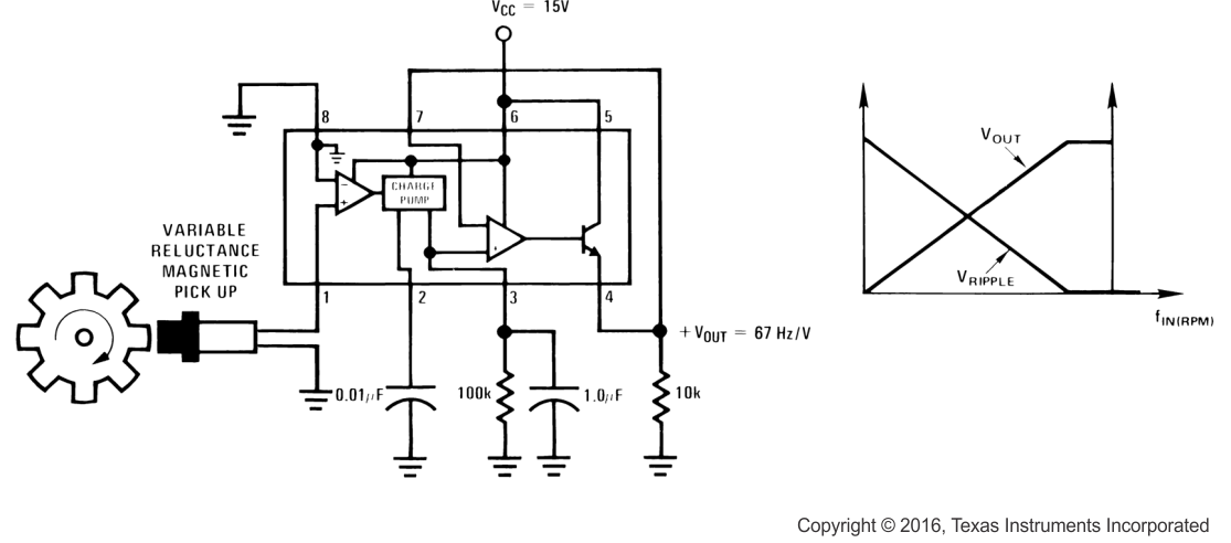 Figure 15. Minimum Component Tachometer Diagram
10.2.1.1 Design Requirements
- C1: This capacitor is charged and discharged every cycle by a 180-µA typical current source. Smaller capacitors can be charged quicker therefore increasing the maximum readable frequency. However, lower capacitors values reduce the output voltage produced for a given frequency. C1 must not be sized lower than 500-pF die to its role in internal compensation.
- R1: This resistor produces the output voltage from current pulses source by the internal charge pump. Higher values increase the output voltage for a given frequency, but too large will degrade the output’s linearity. Because the current pulses are a fixed magnitude of 180 µA typical, R1 must be big enough to produce the maximum desired output voltage at maximum input frequency. At maximum input frequency the pulse train duty cycle is 100%, therefore the average current is 180 µA and R1 = Vo(max) / 180 µA.
- C2: This capacitor filters the ripple produced by the current pulses sourced by the charge pump. Large values reduce the output voltage ripple but increase the output’s response time to changes in input frequency.
- Rload: The load resistance must be large enough that at maximum output voltage, the current is under the rated value of 50 mA.
10.2.1.2 Detailed Design Procedure
10.2.1.2.1 Choosing R1 and C1
There are some limitations on the choice of R1 and C1 which should be considered for optimum performance. The timing capacitor also provides internal compensation for the charge pump and must be kept larger than 500 pF for very accurate operation. Smaller values can cause an error current on R1, especially at low temperatures. Several considerations must be met when choosing R1. The output current at pin 3 is internally fixed and therefore VO/R1 must be less than or equal to this value. If R1 is too large, it can become a significant fraction of the output impedance at pin 3 which degrades linearity. Also output ripple voltage must be considered and the size of C2 is affected by R1. An expression that describes the ripple content on pin 3 for a single R1C2 combination is in Equation 6.

R1 can be chosen independent of ripple. However, response time, or the time it takes VOUT to stabilize at a new voltage, increases as the size of C2 increases, so a compromise between ripple, response time, and linearity must be chosen carefully.
As a final consideration, the maximum attainable input frequency is determined by VCC, C1, and I2 in Equation 7.

10.2.1.2.2 Using Zener Regulated Options (LM2917)
For those applications where an output voltage or current must be obtained independent of supply voltage variations, the LM2917 is offered. The most important consideration in choosing a dropping resistor from the unregulated supply to the device is that the tachometer and op amp circuitry alone require about 3 mA at the voltage level provided by the Zener. At low supply voltages there must be some current flowing in the resistor above the 3-mA circuit current to operate the regulator. As an example, if the raw supply varies from 9 V to 16 V, a resistance of 470 Ω minimizes the Zener voltage variation to 160 mV. If the resistance goes under 400 Ω or over 600 Ω, the Zener variation quickly rises above 200 mV for the same input variation.
10.2.1.3 Application Curves
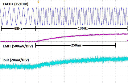
| C1 = .01 µF | C2 = 1 µF | R1 = 100 kΩ |
| Rdrop = 910 Ω | Zener Regulated VCC = 7.58 V | |
in Input Frequency
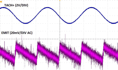
| C1 = .01 µF | C2 = 1 µF | R1 = 100 kΩ |
| Rdrop = 910 Ω | Zener Regulated VCC = 7.58 V | |
10.2.2 Other Application Circuits
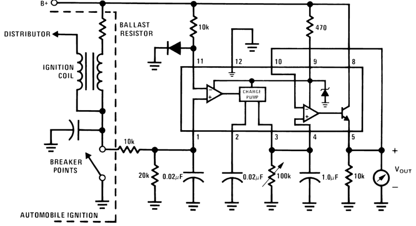
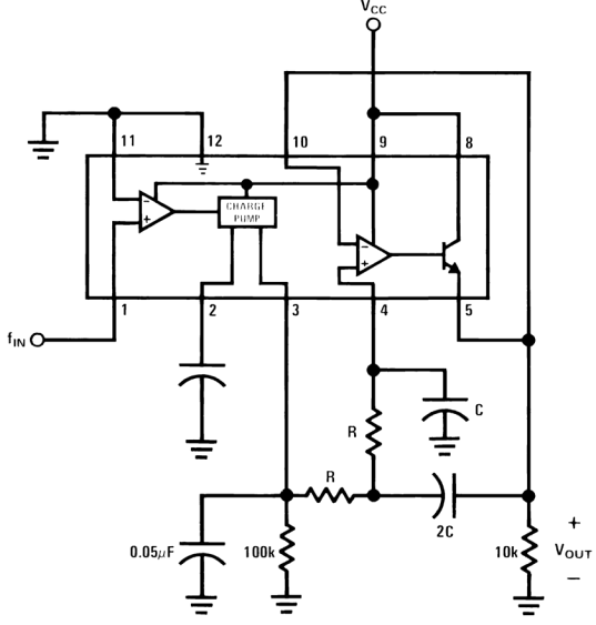
This section shows application circuit examples using the LM2907-N and LM2917-N devices. Customers must fully validate and test these circuits before implementing a design based on these examples.
SPACER
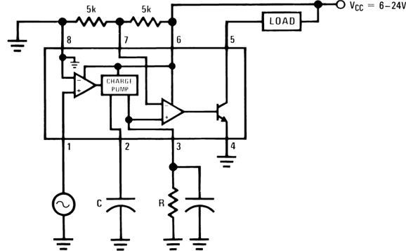
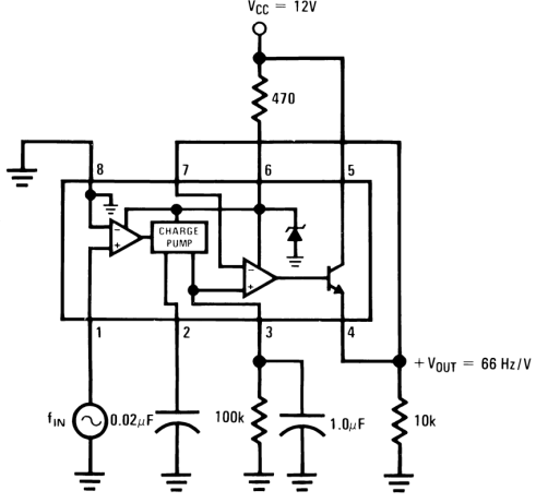 Figure 19. Zener Regulated Frequency to Voltage Converter
SPACER
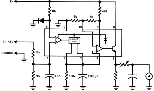 Figure 20. Breaker Point Dwell Meter
SPACER
SPACER
SPACER
SPACER
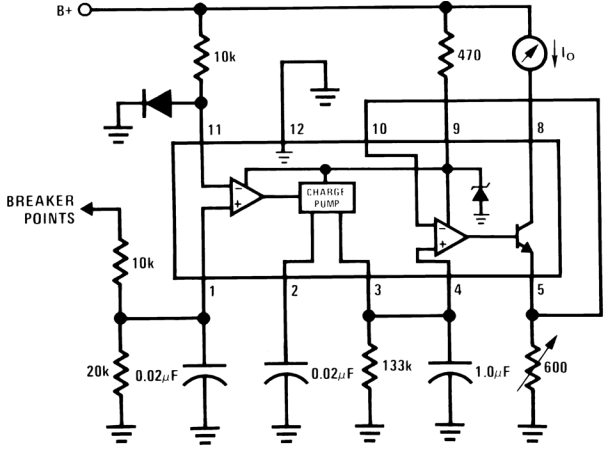
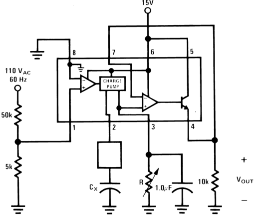
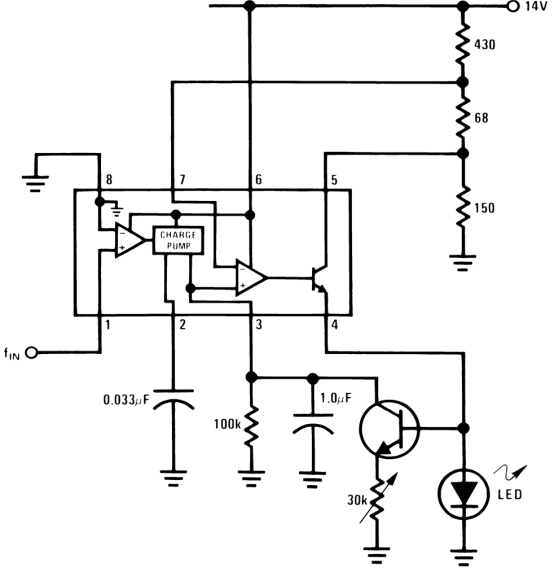
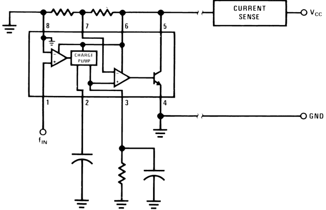 Figure 24. Two-Wire Remote Speed Switch
SPACER
SPACER
SPACER
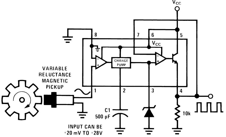
10.2.2.1 Variable Reluctance Magnetic Pickup Buffer Circuits
SPACER
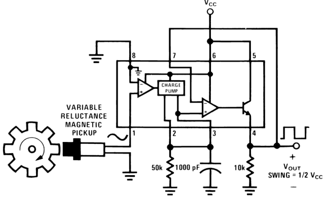 Figure 29. Magnetic Pickup Buffer With 1/2 VCC Output Magnitude
10.2.2.2 Finger Touch or Contact Switch
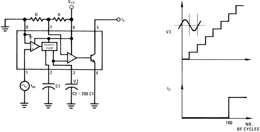
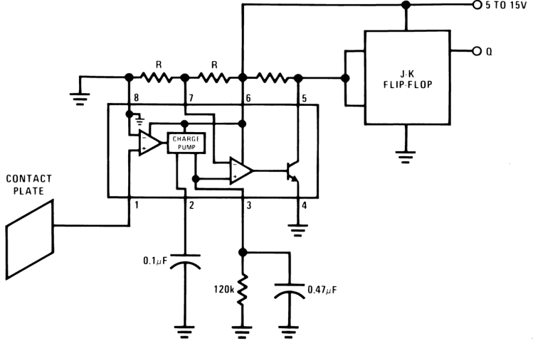 Figure 30. Finger Touch or Contact Switch Diagram
SPACER
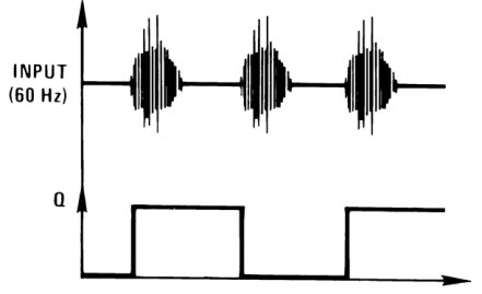 Figure 31. System Output in Response to Consecutive Button Presses
10.2.2.3 Over-Speed Latch
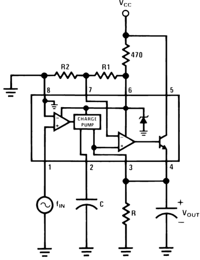
SPACER
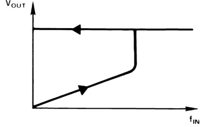 Figure 33. VOUT vs FIN
10.2.2.4 Frequency Switch Applications
Some frequency switch applications may require hysteresis in the comparator function which can be implemented in several ways. Example circuits are shown in Figure 34 to Figure 36.
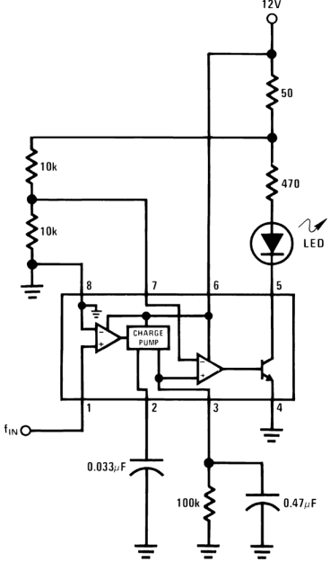 Figure 34. Frequency Switch With Resistor Divider Threshold
SPACER
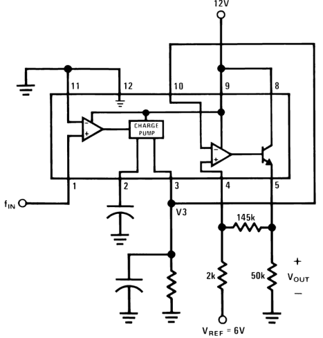 Figure 35. Frequency Switch With Added Hysteresis
SPACER
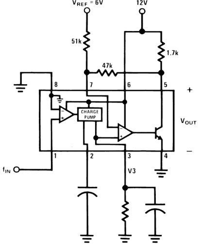 Figure 36. Frequency Switch With Added Hysteresis
10.2.2.4.1 Application Curves
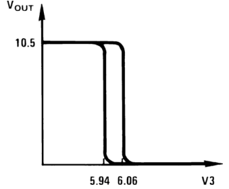 Figure 37. VOUT vs V3
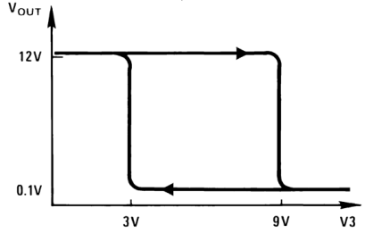 Figure 38. VOUT vs V3
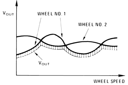
10.2.2.5 Anti-Skid Circuits
10.2.2.5.1 Select-Low Circuit
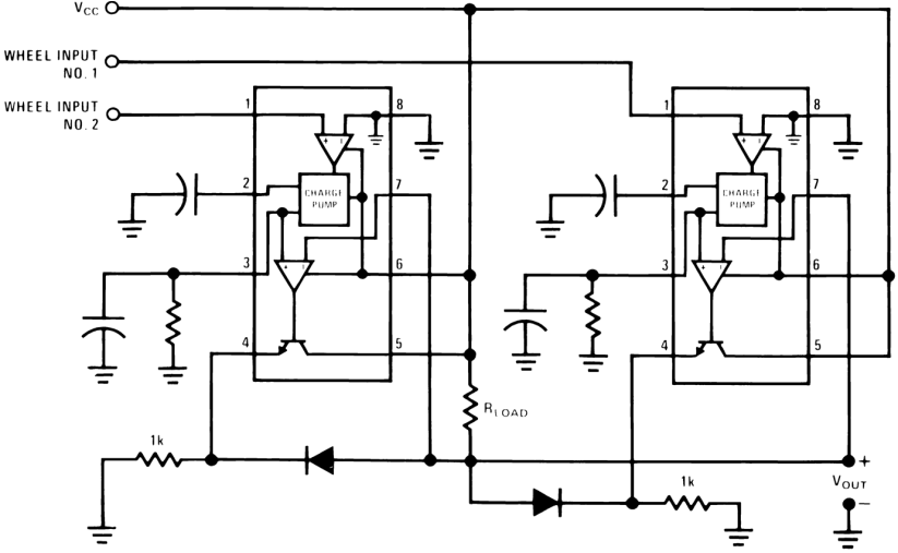 Figure 39. Select-Low Circuit Diagram
SPACER
10.2.2.5.2 Select-High Circuit
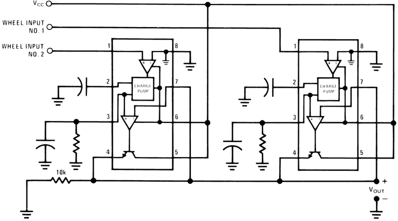 Figure 41. Select-High Circuit Diagram
SPACER
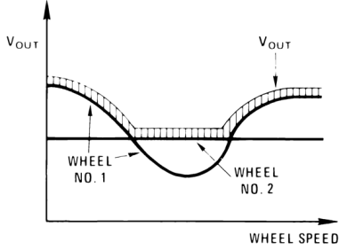
10.2.2.5.3 Select-Average Circuit
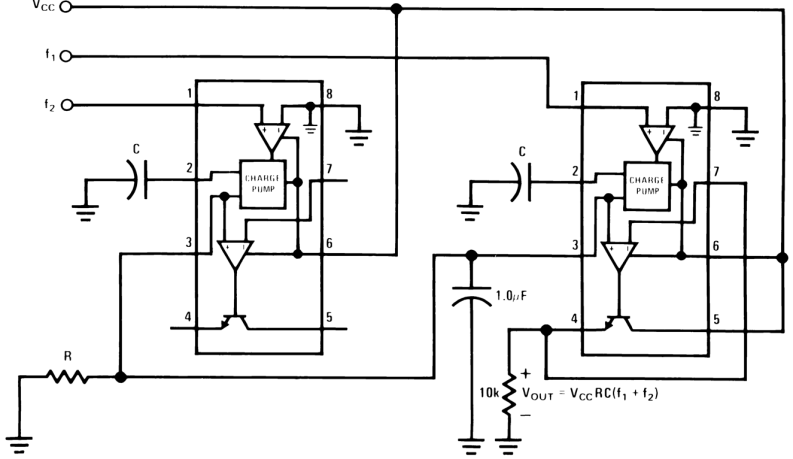 Figure 43. Select-Average Circuit Diagram
10.2.2.6 Changing the Output Voltage for an Input Frequency of Zero
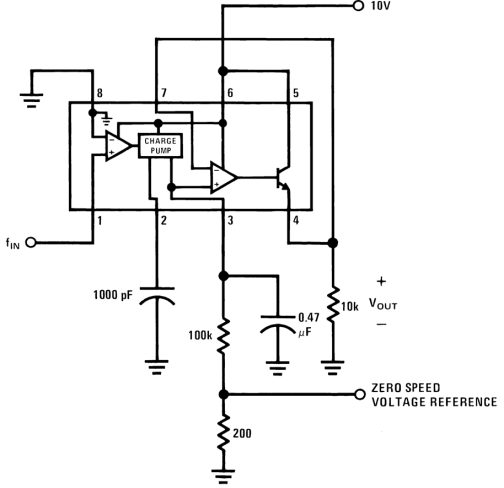 Figure 44. Tachometer With Adjustable Zero Speed Voltage Output
SPACER
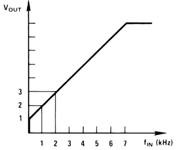 Figure 45. VOUT vs Frequency Plot Shifted to Produce 1 V at Zero Speed
10.2.2.7 Changing Tachometer Gain Curve or Clamping the Minimum Output Voltage
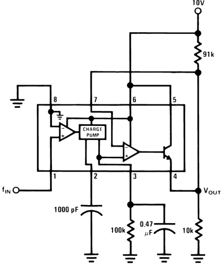 Figure 46. Tachometer With Output Clamped at Low Speeds
SPACER
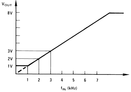 Figure 47. VOUT vs Frequency Plot With Output Clamped at Low Speeds